The output impedance and plate impedance of the MOSFET mu-follower can be analyzed by considering that the MOSFET has an internal source resistance of 1/gfs, which is in circuit between the ideal zero-resistance source and the output source terminal.
Thus the internal source resistance and external source resistance form a voltage divider into, or out of, which the output current flows. This imparts a partial anti-triode like behavior (except 1/gfs is nonlinear) at smaller values of external resistance, as well as allowing the 1/gfs nonlinearity to swamp out desired anti triode behavior in extreme cases. I.e. there is some load current sharing between the tube and MOSFET.
The plate impedance is impacted by the finite gfs because changing output current necessitates a changing g-s voltage across the source resistor. Some fraction of the output signal current is thus "reflected" back to the plate at the ratio of 1/gfs to the external source resistance.
The output impedance is similarly affected because in order to change output current, the voltage across the external source resistor must change, causing a changing current that works into the finite plate resistance of the tube.
The larger the external source resistor, the smaller fraction of the output current reflected back to the tube plate, increasing the impedance seen by the plate and decreasing the output impedance seen at the MOSFET source terminal.
I leave it as an exercise to derive the precise relations...")
Thanks very much, Michael.
I will start from the beginning and try to learn a little about FETs!
Paul
Looks right from the measurements by Gary Pimm.
CCS performance measurments
Thanks Bas, that chart is very informative.
Paul
Paul,
Reading Morgan Jones' book you can get some useful values of the DN2540 to use it in a CCS. The CCS impedance of a single MOSFET is around the setting resistor multiplied by mu (gm*rds). Morgan measured mu from the MOSFET curves as typically rds and gm at the drain current are not specified on the datasheet. For the DN2540 mu is around 4,500 (gm=150mA/V and rds=30K)
Depending on the rset value you need to set the quiescent current, let's say you want to set to 5mA, you need about an rset of 300 ohms, then the output impedance of the CCS is approximately 1.3M. Of course if the CCS is cascoded this impedance can be increased by a factor of rds in theory but you would probably get a CCS with 100Meg or more as the parasitic impedances of the MOSFETs start to contribute here decreasing the impedance of the CCS.
I'm not very knowledgable on this subject, but I think the above rationale is ok, please correct otherwise!
I don't have experience with differential pairs as haven't tried them yet, however I think you need a tail CCS and if you want to balance current on both triodes you need CCS not gyrators as the latter will fix the voltage and with different triodes you will end up with different currents, correct?
So simple CCS or cascoded CCS can be built there if you want to. Can be bipolar ones as perform really well if you don't fancy experimenting with MOSFETs...
Hope this helps?
I have had a good look in MJ's book and cannot find any reference to MOSFETs or to DN2540. Perhaps you have the 4th Edition?
Paul
the whole primm wegbsite has lot to say about regs. Welcome to Gary Pimm's DIY Page
Thanks, but I am trying to find out a)actually what a gyrator does and how it differs from an active load and b) how to calculate the effective output resistance when a mosfet is so used. I looked again at IRF820; this apparently is a "n-channel" device; we have some here. I have no idea if it can be used in the anode circuit of a valve; perhaps I need a p-channel device? I'm afraid I simply don't understand these things despite all the kind help I have received here. The IRF 820 spec says its transconductance is 2.3; since HFE apparently doesn't exist for FETS I don't know what to base my calculations on; but if I have read it correctly 2.3 seems a pretty pathetic value, but then 2.3 what?
Anyway I have no idea if a gyrator is better than the active load or even if there is any real difference. There is talk of the DN2540 but they are costly and apparently difficult to find.
As a result of all this, I think I shall build active loads with MPSA92 a TO-92 PNP transistor, safe to 300V and cheap. I have drawn up the circuit and it should provide me with an output resistance close to 1 megohm which is pretty well exactly what I need.
I would like to know though if a gyrator is better (can I use MPSA92?) and if so, why.
Paul
Last edited:
I have had a good look in MJ's book and cannot find any reference to MOSFETs or to DN2540. Perhaps you have the 4th Edition?
Paul
Yes, should have clarified this. Mosfet CCS are only covered in 4th edition I think.
Paul,
I suggest you read through all previous post recommended first and get a basic understanding of the Mosfet and its characteristics (they do work somehow in a similar way as the valves so should be easier to understand them based on your vast experience with the valves). Mosfets don't have hfe, the have gm (as valves do). Have some similar drain resistance (anode resistance, and particularly the depletion mode ones work just like a valve. At 0V Vgs will conduct and you need a negative (or positive) voltage to turn them off. These are easier to use in an CCS or gyrator from a bias perspective. Read Gary's website suggested above with a lot of good info on this.
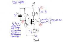
You don't need to use an DN2540. Attached is a very simple PMOS based gyrator with only one transistor. You can use a Zetex ZVP0545a which is easy to obtain around here and is not a surface mount type
Steps to complete the design on this gyrator are the following:
1) First you need to ensure you can bias correctly the Mosfet. Knowing your anode quiescent current (Ia) you can set R5 to ensure bias is stabilised
2) then you have to ensure you keep the mosfet Vds at least 25V to 50V to ensure output capacitance is minimised and performance is achieved. Then R5 can be calculated as well knowing your target Vanode
3) R2 and R3 will set the anode voltage. But also you know the gate voltage based on R4 and Vgs. You can calculate this divider given these two definitions. Also R2 plays with the capacitor to define the rolloff frequency.
Hope this helps a bit...
Cheers,
Ale
I suggest you read through all previous post recommended first and get a basic understanding of the Mosfet and its characteristics (they do work somehow in a similar way as the valves so should be easier to understand them based on your vast experience with the valves). Mosfets don't have hfe, the have gm (as valves do). Have some similar drain resistance (anode resistance, and particularly the depletion mode ones work just like a valve. At 0V Vgs will conduct and you need a negative (or positive) voltage to turn them off. These are easier to use in an CCS or gyrator from a bias perspective. Read Gary's website suggested above with a lot of good info on this.
You don't need to use an DN2540. Attached is a very simple PMOS based gyrator with only one transistor. You can use a Zetex ZVP0545a which is easy to obtain around here and is not a surface mount type
Steps to complete the design on this gyrator are the following:
1) First you need to ensure you can bias correctly the Mosfet. Knowing your anode quiescent current (Ia) you can set R5 to ensure bias is stabilised
2) then you have to ensure you keep the mosfet Vds at least 25V to 50V to ensure output capacitance is minimised and performance is achieved. Then R5 can be calculated as well knowing your target Vanode
3) R2 and R3 will set the anode voltage. But also you know the gate voltage based on R4 and Vgs. You can calculate this divider given these two definitions. Also R2 plays with the capacitor to define the rolloff frequency.
Hope this helps a bit...
Cheers,
Ale
Attachments
Paul,
I suggest you read through all previous post recommended first and get a basic understanding of the Mosfet and its characteristics (they do work somehow in a similar way as the valves so should be easier to understand them based on your vast experience with the valves). Mosfets don't have hfe, the have gm (as valves do). Have some similar drain resistance (anode resistance, and particularly the depletion mode ones work just like a valve. At 0V Vgs will conduct and you need a negative (or positive) voltage to turn them off. These are easier to use in an CCS or gyrator from a bias perspective. Read Gary's website suggested above with a lot of good info on this.
You don't need to use an DN2540. Attached is a very simple PMOS based gyrator with only one transistor. You can use a Zetex ZVP0545a which is easy to obtain around here and is not a surface mount type
Steps to complete the design on this gyrator are the following:
1) First you need to ensure you can bias correctly the Mosfet. Knowing your anode quiescent current (Ia) you can set R5 to ensure bias is stabilised
2) then you have to ensure you keep the mosfet Vds at least 25V to 50V to ensure output capacitance is minimised and performance is achieved. Then R5 can be calculated as well knowing your target Vanode
3) R2 and R3 will set the anode voltage. But also you know the gate voltage based on R4 and Vgs. You can calculate this divider given these two definitions. Also R2 plays with the capacitor to define the rolloff frequency.
Hope this helps a bit...
Cheers,
Ale
Thanks that's very helpful.
A couple of points; by "R5" I suppose you mean R1 and of course the potential divider that determines the anode voltage comprises R2 and R4 in parallel on top of R3. Regarding the capacitor, in quiescent mode there are only five volts across this, but what happens should the valve swing to 0mA and thus the full HT voltage appears across the transistor? I ask because I have very little space for four anode loads and a 1uF capacitor at any kind of serious voltage would be much too large.
Finally I suppose that output resistance is calculated by multiplying R1 by the gm?
One more thing, I see that no value for gain is given in the specification of the ZVP0545A; how is this determined?
Paul
Last edited:
More on CCS
More reading material, as usual Pete Millett has a good write-up here. So does Tubelab.
Jaz
More reading material, as usual Pete Millett has a good write-up here. So does Tubelab.
Jaz
Thanks that's very helpful.
A couple of points; by "R5" I suppose you mean R1 and of course the potential divider that determines the anode voltage comprises R2 and R4 in parallel on top of R3. Regarding the capacitor, in quiescent mode there are only five volts across this, but what happens should the valve swing to 0mA and thus the full HT voltage appears across the transistor? I ask because I have very little space for four anode loads and a 1uF capacitor at any kind of serious voltage would be much too large.
Finally I suppose that output resistance is calculated by multiplying R1 by the gm?
Paul
Ops. I meant R4 instead of R5 (it doesn't exist!)
R2 and R3 are the only resistors setting the gate voltage. R4 doesn't interact as a resistor in parallel with R4 as the gate is very high impedance (remember the characteristic of the mosfet).
Unfortunately the capacitor should be able to support the HT swing
Regarding output impedance. Mm, someone can help here but it should be gm*ro*R4 + R1 in parallel with R3 +Xc1? Someone can please confirm this?
BTW: If you're still looking at using this in your differential pair, I think you should be looking at a CCS instead as you need to maintain constant current, not voltage as in the Gyrator...
Mixed up R5 with R4 and R1 so it's really confusing so here goes again:
Steps to complete the design on this gyrator are as follows:
1) First you need to ensure you can bias correctly the Mosfet. Knowing your anode quiescent current (Ia) you can set R4 to ensure bias is stabilised as shown in the diagram (point 1)
2) You then have to ensure you keep the MOSFET Vds at least 25V to 50V to ensure output capacitance is minimised and expected frequency response performance is achieved. Then R1 can be calculated as well knowing your target anode voltage (Va), Vds and voltage drop across R4 and +B. (point 2)
3) R2 and R3 will set the anode voltage (Va) which is a design parameter in the gyrator, right?. And also you know the gate voltage (Vg) based on R4 and Vgs (i.e. +B-VR4-Vgs). You can calculate this resistor divider given these two definitions. Also R2 plays with the capacitor to define the rolloff frequency of your gyrator.
Sorry for the confusion!
Ops. I meant R4 instead of R5 (it doesn't exist!)
R2 and R3 are the only resistors setting the gate voltage. R4 doesn't interact as a resistor in parallel with R4 as the gate is very high impedance (remember the characteristic of the mosfet).
Unfortunately the capacitor should be able to support the HT swing
Regarding output impedance. Mm, someone can help here but it should be gm*ro*R4 + R1 in parallel with R3 +Xc1? Someone can please confirm this?
BTW: If you're still looking at using this in your differential pair, I think you should be looking at a CCS instead as you need to maintain constant current, not voltage as in the Gyrator...
No, I explained earlier, I use a cascode CCS in the tail of the differential pair; this has an AC resistance of about 30 megs. The idea is to use active anode loads in place of the 97k resistors that are there at present.
I think I mentioned I once built a differential driver stage using a 7N7 with pentode cathode follower (E810F). The 7N7 had active loads and of course a CCS in the tail. The E810F had a CCS load and also an active g2 supply linked to the cathode. I tested the prototype and got 77.5v rms out at 0.06%THD. The active loads on the 7N7 were just MJE350s. Obviously the anode load resistance must be substantially less than the tail resistance, otherwise the diff. pair simply wouldn't work; this is why I want about 1Meg or so, enough to give me flat AC loadline without upsetting the operation of the diff pair.
I saw gyrators mentioned and wondered if they would perform better than the active loads I have previously used. It seems that I may have to use the active loads as I have not really got space for anything more complex.
Thanks
Paul
- Status
- This old topic is closed. If you want to reopen this topic, contact a moderator using the "Report Post" button.
- Home
- Amplifiers
- Tubes / Valves
- Gyrators