What is the best strategy with planes in an offline SMPS?
3 grounds:
a) Earth.
b) Power.
c) Circuit.
On the line side, there's Earth ground for safety, which I would expect to simple connect from the Earth power-prong to the Y-caps.
Power ground, as I am calling it, is really the line-side common that is after the bridge rectifier. It is likely a diode rise over the Power-Neutral, which sort of gets grounded to Earth (I think) back at the circuit breaker.
Circuit ground, in this application, is the output voltage common. It floats, but can be connected to the rest of the circuit grounds.
I'm not sure if that's clear or not?
Does it make sense that the PCB should have one continuous plane, and it be one of these grounds? If so which? I think circuit ground.
If that isn't okay, then how to best make ground planes on the PCB?
I think a lot of folks use 2-layer PCB for SMPS, but isn't it better to use 4?
In prior designs, I had a split ground plane. One half is line-side power ground. The other half is circuit ground. The 2 do not connect on the PCB and the split occurs at the power transformer. So I wonder if that leads to trouble with either coupling noise, or possibly ground loops.
Any thoughts?
FWIW ... I have designed a few PS modules for audio (and am a PCB Design Engineer by trade) and here is my take:
1. Only put AC line & neutral on the PCB and make sure to follow the IPC guideline for spacing for 250VAC (I always double the voltage to be safe hence 250V vs 120V).
2. I do not connect Earth GND to the PCB unless I have a thermistor or some sort of ground lift circuit. Even then it is a trace and not a plane.
3. I do NOT extend GND plane under any of the AC lines or components. Remember that clearance applies in the Z-axis also.
4. For SMPS, it depends ... are you laying out the circuit or utilizing a module? If you are laying out a circuit, you need to make sure the noisy switchnode between the switching device and the inductor is as short as possible and there is solid DC GND under it in the form of a plane. Also keep a contiguous path between input cap and output cap GNDs either on the top or bottom side. For SMPS, I typically flood both sides with GND and tie with vias but keeping the above in mind. The smallest caps go closest to the switching device. If it is an SMPS module, most of those are shielded, so then just make sure that every trace has a return path. The easiest method is route all traces on the top and put a solid GND plane on the bottom.
5. Put your GND point that will tie to the device star GND as close to the last bulk cap in the supply as possible. This is where the bulk of the current will return. I usually do NOT ground the mounting screws but rely on the Star GND point to eliminate any potential GND loops.
6. If I am routing circuitry on the same PCB, I will still use one GND plane by again trying to "steer" the current back to that last cap in the PS filter. You can do this by cutting slots in the plane, using a thick trace to join the 2 planes at that point or even use a jumper wire. Just make sure no traces cross that slot or gap.
Yes, I'm laying out myself.
I plan to use Earth ground for transient suppression return, so it'll at least be a short trace from plug to suppression devices.
Yep, I understand about the clearance layer to layer.
So no planes under the AC lines? Okay, but after the full-bridge rectifier, and the big bulk decouple caps, from there on I call the common point "power ground". In your explanation, this plane goes under all the PWM and associated parts, yes?
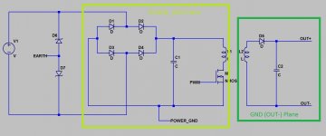
Here is a very simple smps. It shows the output floating, but either OUT- or OUT+ can be grounded. Are you saying that you connect POWER_GROUND to OUT-?
I plan to use Earth ground for transient suppression return, so it'll at least be a short trace from plug to suppression devices.
Yep, I understand about the clearance layer to layer.
So no planes under the AC lines? Okay, but after the full-bridge rectifier, and the big bulk decouple caps, from there on I call the common point "power ground". In your explanation, this plane goes under all the PWM and associated parts, yes?
Here is a very simple smps. It shows the output floating, but either OUT- or OUT+ can be grounded. Are you saying that you connect POWER_GROUND to OUT-?
An externally hosted image should be here but it was not working when we last tested it.
Looking at this diagram, you are using coupled inductors so there is no need to tie POWER_GND with "signal ground" or OUT-. I would have an isolated POWER_GND plane under the primary side and an OUT- "signal ground" plane under the secondary side. If you need to feed the PWM signal from a sense circuit on the secondary side, you may want to use an opto-isolator across the gap.
Attachments
One of the main reasons to use a ground plane is that they have low impedance. They have low impedance because they reduce loop area by allowing current flowing through a conductor to return directly underneath it through the ground plane. Thus, if your circuit consists of two halves where current never flows from one half to the other, then you don't need to connect the grounds between them.
- Status
- This old topic is closed. If you want to reopen this topic, contact a moderator using the "Report Post" button.