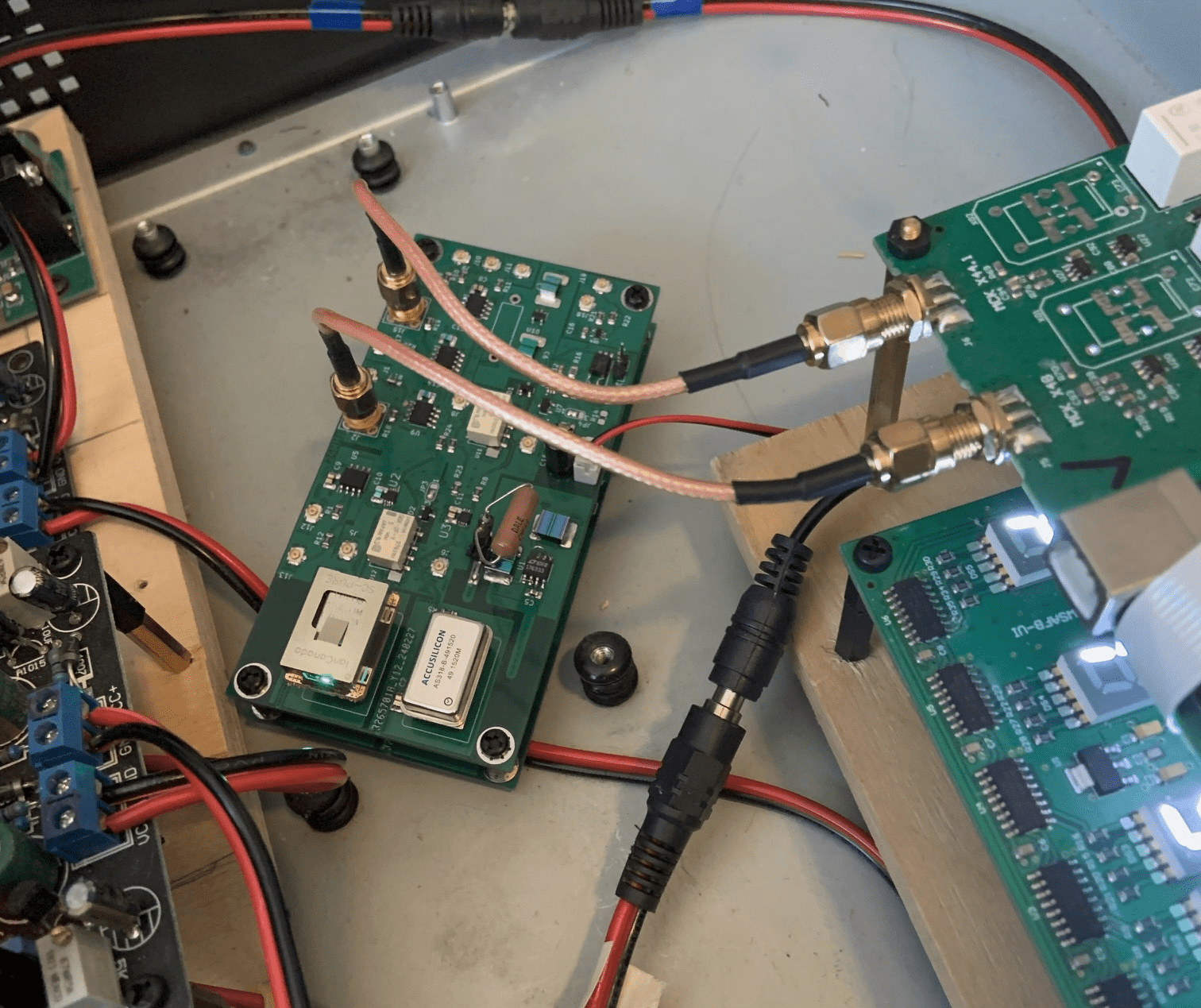
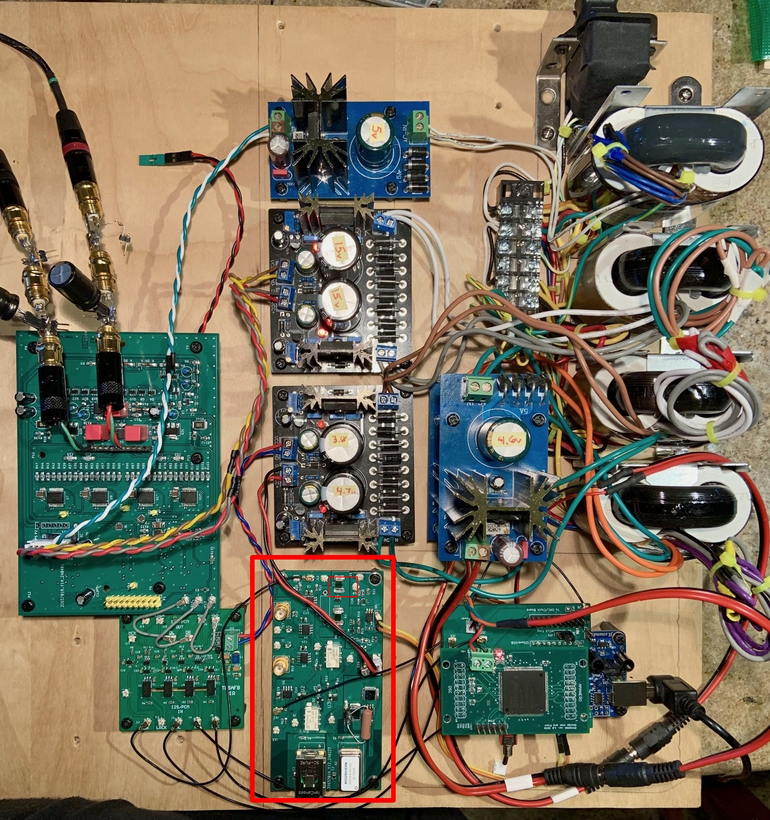
Some pics of a prototype general purpose DAC Clock board, for which I plan to post the Kicad project. First pic is driving a Andrea Mori FIFO Buffer board; second pic is driving a @MarcelvdG RTZ FIRDAC with asynchronous USB, and reclocking before the dac board (clock board prototype is outlined in red).


At this point the premise is that the clock board will use 45/49MHz clock modules (or external clocks, including sine wave oscillators using suitable squaring adapters). The 45/49MHz frequencies can be used to externally clock an I2SoverUSB board. The clock frequencies are then divided by two to produce 22/24MHz clocks for driving dacs. Both continuous and switched 22/24MHz outputs are available (USB board usually controls the switching). All outputs are buffered with high performance buffers. Very clean +3.3 power distribution and bypassing is also used. That's the short story.
One thing still thinking about is that some people might prefer to use 22/24MHz clocks to begin with, then use a frequency multiplier to drive the USB board (as an option).
So, a couple of questions would be as to how much interest there would be in a board like this (in the form of an open source Kicad project), and whether or not making the board slightly longer to accommodate an optional frequency multiplier would be preferred.
So far with the prototype and some pretty good clocks, it does raise the DACs in the pics into what I would consider to be a higher sound quality performance league as compared to what they would sound like with off the shelf NDK SDA, Accusilicon, and or Crystek (although the clock board can make those clocks sound better too), and or especially better if compared to having the master clocks internal to the USB board.
Of course, all the above having been said, there are commercial solutions out there too. Some are essentially SOA, but they may be more costly and possibly less adaptable than the clock board of this project.
Last edited:
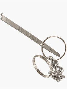
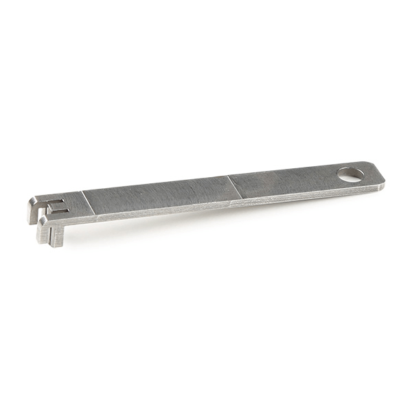
A couple of recommended tools for use with u.fl cables:
Puller tool helps extend connector life:
https://www.mouser.com/ProductDetai...AqNu8ARuPVMTDmAzZO30VhJWZTxV2LEBoCyJIQAvD_BwE

Sparkfun push/pull tool can help with installing connectors in tight spaces:
https://www.sparkfun.com/products/20687

Puller tool helps extend connector life:
https://www.mouser.com/ProductDetai...AqNu8ARuPVMTDmAzZO30VhJWZTxV2LEBoCyJIQAvD_BwE
Sparkfun push/pull tool can help with installing connectors in tight spaces:
https://www.sparkfun.com/products/20687
Hi Randy,
You are very welcome, of course
Right now a 2nd prototype is at jlcpcb. It mostly differs from the first prototype in the model of buffers used. First prototype used NB3L553-D; the second one uses LMK1C1104. A few other changes as well. After deciding if one buffer type is preferred over the other, then maybe another version to fix any problems that turn up, and or maybe to add a multiplier.
Mark
Randy,
So far the SMA connectors are there for convenient connection to Andrea's boards, since he uses SMA. They are kind of big and costly for all the little optional connectors though.
Anyway since this is an open source project, once anyone sees how it works then it shouldn't be too hard to modify it for SMA connectors in key places. Most of the outputs run along the edges, so the board could easily be widened to make space for them. There are also some u.fl connectors more in the middle of the board, but those are ones I wouldn't expect to be used much. Those are mostly for doing things like experiments such as to see how much difference buffers or their absence makes to dac performance. They could also be used as inputs, but most people probably wouldn't want to use them for that most of the time.
Mark
EDIT: Probably I will add a multiplier since its easy to do. However things like that then raise other questions, like should there by solder jumpers to bypass the dividers in case 22/24MHz clocks are used? Probably. But there isn't much space left to add more feature creep without significant layout changes in the middle of the board. However, will take a look at it after trying out the new boards.
Last edited:
Hi Mark ... & thanks for sharing this. Still thinking that it looks very neat 
One comment & a question, the comment first: I notice that you consider adding a clock multiplier, however, have you considered that e.g. the JLSounds board's PLL may then lock on to either of the two edges being generated by the multiplier for each 22/24 MHz oscillator clock edge? In my experience this may be challenging to solve (others may of course be better at this) ... An alternative - at least for those using the JLSounds board - may be to have JLSound replace the firmware for a 22/24 kHz version, thus omitting the need for a clock multiplier altogether.
And then the question: You are considering the LMK1C1104 as an alternative to the NB3L553 ... Can I ask you why? At least in the datasheet the LMK** does not have any information about close-in phase noise performance ...
Cheers, Jesper
https://www.diyaudio.com/community/threads/return-to-zero-shift-register-firdac.379406/post-7663201At least in the datasheet the LMK** does not have any information about close-in phase noise performance ...
@bohrok2610: Many thanks for linking ... My mistake actually - I do remember from the RTZ thread that you mentioned it earlier ... BTW, it looks like a very interesting device and also at a very reasonable price ...
Cheers, Jesper
Cheers, Jesper
Hi Jesper,...have you considered that e.g. the JLSounds board's PLL may then lock on to either of the two edges being generated by the multiplier for each 22/24 MHz oscillator clock edge?
To answer your question, Yes. Doesn't usually seem to happen, but it can happen at I2SoverUSB whether the 45/49MHz clock signal going to I2SoverUSB is from the crystal oscillators or from a multiplier. The place to deal with it is probably in or just before the reclocker board. Since we have both the 45/49MHz and the 22/24MHz clocks available at the clock board, if we send both clock signals over to, say, the reclocker board, we can check to see if BCLK from I2SoverUSB is aligned correctly for reclocking. If not, we can delay the I2S signals using the 45/49MHz clock to realign the I2S properly with the 22/24MHz reclocking signal (or something more or less like that). A short FIFO might be needed, or maybe just some flip-flops and glue logic. Thing is, reclocking is so valuable that we need to solve the problem, so we will just have to figure it out.
The other thing is that folks may need a way to interconnect I2SoverUSB and PCM2DSD, as well as a way to connect clock and I2S bus signals to those two devices. I have an interconnect board for that, so it will probably get thrown in with the clock board open source project.
Cheers,
Mark
EDIT: Regarding the PLL question, also occurs to me that the PLL signal could be checked against the 22/24MHz signal while still on the clock board. If the wrong phase, then the PLL output could be inverted before leaving the clock board. We'll see.
Last edited:
Thinking a little more about the PLL issue, maybe all that's necessary is to add a fractional period delay to the PLL output, say, maybe an RC delay then a buffer (or the equivalent). Why? IIUC there is only a problem if the 22/24MHz reclocker signal edge happens to line up with the BCLK edge (and or other I2S bus edges). Then the output of the reclocker is ambiguous. However, if all we need to do is make sure the edges never exactly line up, then we only need to slightly time shift one of the signals. We don't want to mess with the reclocker timing, so we should time offset the PLL output a little. Make sense?
Last edited:
They are all effectively synchronous signals. They all originate from the same master clocks on the clock board. They are just sometimes in unfortunate phase relative to each other. Not a big problem to fix.
Also, we want to use the 22/24MHz signals for reclocking since they have about 6dB less phase noise than the 45/49MHz master clocks (if that's what we are using).
Also, we want to use the 22/24MHz signals for reclocking since they have about 6dB less phase noise than the 45/49MHz master clocks (if that's what we are using).
Boards for that are available from TheWellAudio. That's what I use anyway.
Just to be clear, I am okay with designing and giving away some things that aren't otherwise readily available. What I am trying to do is advance the art of dac building for more people in the diy world. However, for things that are already accessible then I don't see why I need to fill a gap there. That said, if TheWellAudio (for example in this case) or other folks can't supply parts you may like to have, then maybe I would consider doing a little more design work for free. However, I'm hoping that once people see how this type of thing can be done then more people will feel comfortable doing more of it themselves.
Just to be clear, I am okay with designing and giving away some things that aren't otherwise readily available. What I am trying to do is advance the art of dac building for more people in the diy world. However, for things that are already accessible then I don't see why I need to fill a gap there. That said, if TheWellAudio (for example in this case) or other folks can't supply parts you may like to have, then maybe I would consider doing a little more design work for free. However, I'm hoping that once people see how this type of thing can be done then more people will feel comfortable doing more of it themselves.
Last edited:
IIUC that's the case when the original I2S clocks are generated from the MCLK. But why reclocking then if the MCLK is what makes the codecs tick?They are all effectively synchronous signals. They all originate from the same master clocks on the clock board.
For codecs with MCLK input typically the phase of MCLK vs. I2S clocks is not important, often stated in their datasheet. There may be exceptions though, any cases known?They are just sometimes in unfortunate phase relative to each other. Not a big problem to fix.
Last edited:
The problem was described in another thread by Jesper, then some comments from me:But why reclocking then if the MCLK is what makes the codecs tick?
https://www.diyaudio.com/community/threads/return-to-zero-shift-register-firdac.379406/post-7460443
https://www.diyaudio.com/community/threads/return-to-zero-shift-register-firdac.379406/post-7461516
https://www.diyaudio.com/community/threads/return-to-zero-shift-register-firdac.379406/post-7464286
https://www.diyaudio.com/community/threads/return-to-zero-shift-register-firdac.379406/post-7464432
Basically, it is desired to have a fully synchronous USB dac system (using asynchronous USB), which also is protected from EMI/RFI, and which operates with very low phase noise.
It requires clocking the USB with an external clock so the dac system can be synchronous. Then it requires cleaning up conducted EMI/RFI from the USB board, cleaning up jitter from the USB board, and restoring the ultra-low phase noise of the master clocks before the I2S signals go into the dac board. The reclocker/isolator board is to help with the latter requirements.
However, the USB board can lock onto the 45/49MHz clock signal at two different times relative to the 22/24MHz clock frequencies from the clock board (both 45/49MHz and 22/24MHz clock signals originate from one set of physical clocks on the clock board). Depending on which relative time the USB board is operating at, the 22/24MHz clock signal may or may not be in the right relative phase for reclocking to work in order to remove jitter and restore low phase noise. That's the problem.
The solution may turn out to be as described above in #11.
Last edited:
Thanks. But still I do not understand why the need for reclocking. IIUC - the precise clock feeds MCLK to the async UAC2 receiver to generate I2S and at the same time MCLK for the codec. Why reclocking the bclk/lrclk I2S clock signals? But I may be getting something wrong, thanks 
In the case of Marcel's RTZ FIRDAC, it is clocked by BLCK from the USB board and or from PCM2DSD. BCLK is dirty by the time it gets to the dac and there is EMI/RFI noise on it. Reclocking and isolation makes it good.
It also turns out that some dac chips, ASRC chips, dac boards, etc., tend to produce cleaner output with cleaner incoming BCLK and or LRCK signals. Thus isolation and reclocking can often be helpful for those dacs too. DATA signals from the USB board may not as critical in terms of timing, but removing common and or differential conducted EMI/RFI noise from the USB board can also often be helpful.
Another consideration is the isolators add some jitter. If we don't want the added jitter but we do want the isolation, then its easy to define a standard signal conditioning process that is used before I2S signals go into the dac board. The standard process I use is isolation followed by reclocking. Experimental evidence is that it helps to use such a process. It also helps to baby the clocks as much as possible if the lowest phase noise is desired. When its all done well enough, then its quite obvious that humans can hear significantly lower levels of jitter than old literature may seem to suggest. However, and as always, thresholds such as the threshold of audibility for jitter are not hard limits. They are estimates of the center of a bell curve. There are no doubt some people who are closer to the right side tail. These people may hear the effects of very low close-in phase noise (which is mainly soft-sounding, audio-signal-correlated 1/f noise). IME the 1/f noise buries/hides/masks some of the low level musical details.
Last edited:
OK, that makes sense, no MCLK for the DAC, the conversion is clocked by BCLK.In the case of Marcel's RTZ FIRDAC, it is clocked by BLCK from the USB board and or from PCM2DSD.
For ASRC it obviously makes sense because BCLK enters the ASRC calculation. But why ASRC if precise MCLK and synchronous I2S is available? Are there any measurements or test data showing this improvement for no-ASRC chain with proper MCLK input too? Thanks.It also turns out that some dac chips, ASRC chips, dac boards, etc., tend to produce cleaner output with cleaner incoming BCLK and or LRCK signals.
Actually technically the most simple method would be MCLK -> codec being I2S master -> USB receiver being I2S slave. But it requires to have control over the USB receiver setup which often is not the case, using the closed ready-made boards.
Last edited:
- Home
- Source & Line
- Digital Line Level
- General Purpose DAC Clock Board