I don't think there would be any benefits, no.Would there be any benefit in adding a small series resistor in series between the diodes and the first (ripple) cap, if that could be easily tried?
If the dropout voltage and the value of the main ripple cap are selected correctly, there is essentially no ripple at the output, and close to zero other noise. It will also increase the likelihood of radiated noise at the occasional high-current peaks, especially if one were to mount one vertically, which is sometimes done to save space.
Btw, I will look for any ringing again, when I get some of the MSR860's, but if I don't see any now, I doubt it will change.
I assume you mean use the board as a CM filter only, after your power supply?? If that is the case you should not have any problems, because the ripple will already be low, so the dropout voltage can be set at a normal low-ish level.I am dual secondarys at this point, and will be looking to splice in post rectifier for the CM benefits initially.
There are faston connectors on the side of the board that can be used either as a DC input (if the AC input to the bridge rectifier is not being used), or as an unregulated output. This was done to accomodate separate supply feeds to the front and power stages of VSSA if desired, but you could use it for your purposes.
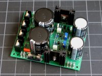
The heatsink at the pass transistor is rated at 11C/watt, and there are larger and smaller versions available to fit the same footprint.
So for example, say you want to plan on 2A average, and the ripple in your power supply is already low, so you set the dropout to 1V (or less). The pass transistor will dissipate 2 watts, and the heatsink temperature rise will be about 22C above your internal chassis temperature.
Can you post what your supply looks like now, and how much ripple is left on the output?
Sorry for the cryptic post.
I have dual secondarys>rectifier set with their own heatsinks>CLCLC>F5
I have about 1.3V ripple post rectifiers,10-12 mV post filtering. This is quiescent. It works well and sounds good, but is not elegant or even sane.
I finally need to see what difference a CM would make, and see if I can shed a few heavy inductors. Or caps even.
I did see your faston's as DC input. One of many reasons I like your layout.
Why did you choose gold-plated contacts vs tin- or solder-plated?
Not a widespread issue in DIY, I should think, but the advantages of gold are not harnessed in this application.
http://www.semlab.com/goldembrittlementofsolderjoints.pdf
Not a widespread issue in DIY, I should think, but the advantages of gold are not harnessed in this application.
http://www.semlab.com/goldembrittlementofsolderjoints.pdf
Last edited:
Don't shed too many...Sorry for the cryptic post.
I have dual secondarys>rectifier set with their own heatsinks>CLCLC>F5
I have about 1.3V ripple post rectifiers,10-12 mV post filtering. This is quiescent. It works well and sounds good, but is not elegant or even sane.
I finally need to see what difference a CM would make, and see if I can shed a few heavy inductors. Or caps even.
I did see your faston's as DC input. One of many reasons I like your layout.
")
I tested with ~1V ripple, and as long as the dropout voltage is set high enough, there is nothing measurable/audible on the output, down to about 10mV (where my oscilloscope becomes useless). Basically what I did was leave the amplifier boards connected, and then load the outputs until the current and ripple was about where I wanted, using multiple 100W light bulbs.
Not sure if that is in reference to the power supply board... no gold plating on this one. If you are referring to my through hole VSSA boards, the board house threw that in for free, probably ran my small batch with a different order. Color may be off a bit in the PSU pics. I think I am using the default color correction when I crop and edit them. Board is just conventional tin-over-copper.Why did you choose gold-plated contacts vs tin- or solder-plated?
Not a widespread issue in DIY, I should think, but the advantages of gold are not harnessed in this application.
http://www.semlab.com/goldembrittlementofsolderjoints.pdf
In either case, thanks for posting the link, interesting!
Sorry, the contacts looked gold in the pics you posted.Not sure if that is in reference to the power supply board... no gold plating on this one. If you are referring to my through hole VSSA boards, the board house threw that in for free, probably ran my small batch with a different order. Color may be off a bit in the PSU pics. I think I am using the default color correction when I crop and edit them. Board is just conventional tin-over-copper.
In either case, thanks for posting the link, interesting!
Yes, they do, the color of some of my pics is off, b/c some are taken by daylight, some under incandescent light, some w. flash. Good chance I forgot to correct the color, t/y for pointing it out.Sorry, the contacts looked gold in the pics you posted.
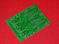
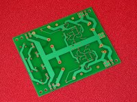
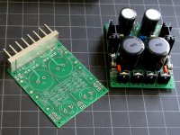
Capacitance Multiplier Schematic & BOM
The attachments are for the circuit board as tested and discussed above.
Not including the boards already sent out, spoken for, or used for testing, there are 5-6 left, and I plan to reorder at least once for those who expressed their interest earlier in this thread and elsewhere. With any luck, the cost will stay $10 plus shipping. Only exception would be if the discount I am using to order small lots were to end.
I will read through the thread and post a list of names later today. Anything after the next small order might have to move to a separate thread in the GB section. MrEvil has graciously let me use this thread so far, and I don't want to abuse the priviledge. (Thanks)
I also plan to publish a version of the layout for a diy etched single layer board in a separate post.
Attachments
The maximum voltage with the components I am using now is +/-50V. You could push this a bit, but not much. As the BOM stands, the limit is given by the MOSFET used as the pass transistor, rated at 55V. At startup, the unregulated output of the rectifier will show up across the pass transistor, and then gradually diminish until it reaches the equivalent of the dropout voltage plus 1/2 the unfiltered ripple.Maybe this has been asked before, but what is the reasonable limit on power on this board, in terms of either voltage or current (ripple, etc.)?
The maximum tolerated ripple will be given by the spec of the large cap after the recifier that you select. The ripple at the output was essentially unmeasurable (read back in the thread, I posted some examples w. scope screen shots).
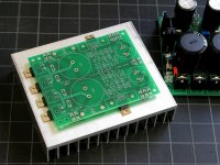
Maximum DC current is likely to be around 5A, limited by the power dissipation of the pass transistor and the size of the heatsinks. The board is also designed to allow the rectifier diodes and pass transistors to mount from the bottom, leads bent @ right-angle, for more heatsink capability (not tested, but see below for the general concept)
Other combinations of components and heatsinks are also possible, as in the second pic.
Attachments
Thanks Pete, could I ask for 2 brds, not one, if available, please.
Also, for changing diodes after the caps are fitted (for people like me!) we can just drill out clearance holes in the heatsinks and use bolt/nut/washer/pad - no problems.
Curiously, Miles' original brds had a separate ground connection for the input power supply caps and another for the rest of the circuit's 0 volt points - not good?
Why are there so many grounds? Doesn't it make sense to use a star at the "output" of this board?The maximum voltage with the components I am using now is +/-50V. You could push this a bit, but not much. As the BOM stands, the limit is given by the MOSFET used as the pass transistor, rated at 55V. At startup, the unregulated output of the rectifier will show up across the pass transistor, and then gradually diminish until it reaches the equivalent of the dropout voltage plus 1/2 the unfiltered ripple.
The maximum tolerated ripple will be given by the spec of the large cap after the recifier that you select. The ripple at the output was essentially unmeasurable (read back in the thread, I posted some examples w. scope screen shots).
Maximum DC current is likely to be around 5A, limited by the power dissipation of the pass transistor and the size of the heatsinks. The board is also designed to allow the rectifier diodes and pass transistors to mount from the bottom, leads bent @ right-angle, for more heatsink capability (not tested, but see below for the general concept)
Other combinations of components and heatsinks are also possible, as in the second pic.
Do you do this often James?....Also, for changing diodes after the caps are fitted ...

The diode heatsinks don't have to be soldered to the board, the diodes, yes, but not the heatsinks...
If you know that is a possibility, just insert the hold-down pin in the board, but do not solder it.
Later, heat the soldered diode leads from the bottom of the board, and pull, the diode can stay attached to the heatsink. The heatsinks I had on hand don't even have the support pin. I like that feature, but you don't have to have it.
Or just get a small offset screwdriver, there is actually about 15 mm to work with... if you can't find one small enough, you can make one out of a pair of old tweezers, just file the tip a little, and then bend it in a vise. Tweezers are usually hard enough to use as a small screwdriver, but soft enough to bend and file.
edit:
Yes, the original layout had a split ground plane, but that is something I did not need in my case. I also made the output cap much larger, because the power supply has to serve the full bandwidth of the amplifier, not just a subwoofer, so current peaks can be much sharper.
Last edited:
Yes, a star ground always makes sense, but people often do not agree on where each individual return should be connected. So, I added a few extra ground points.Why are there so many grounds? Doesn't it make sense to use a star at the "output" of this board?
You only need to install FASTONs where you intend to use one. For testing, I installed all of them.
Basically, there is one for each power take-off connection.
The ones at the unregulated power connections have an addition purpose, they can be used as an extra connecting point for a split supply (still trying to work out if that makes sense for VSSA)
Yes, starting to make the list tonight.Dear PMI,
Can you put me down for Two Boards?
gannaji.
Yes, starting to make the list tonight.
Is it correct that for a stereo VSSA (LC) amp +/- 35V, one PSU board is sufficient? In that case one PCB is sufficient for me. Else, Two Boards. Sorry for the misunderstanding.
--gannaji
- Status
- This old topic is closed. If you want to reopen this topic, contact a moderator using the "Report Post" button.
- Home
- Amplifiers
- Power Supplies
- Finished capacitance multiplier