So this really was just an experiment for fun rather than building something with amazing performance. I was playing around with the chopper JFETs (J112) that have Vgs 3~4V, too high for normal circuit design. I read about the Bastode input stage (here and here) and thought it could give me some fun time, and also no article talked about its properties, so I'd like to share it.
Bastode is really just another kind of differential input stage. In a normal Long-Tailed Pair (LTP), two low impedance pins of the same transistor type are tied together. In a Bastode however, low impedance pins of the opposite transistor types are connected:

Q1 is an Nch-JFET, and Q2 is a Pch-MOSFET. This offers some simplicity: there's no additional current source. The two input transistors decide standing current on their own (which means you have to test it yourself). From the samples of J112 and ZVP2016A I have, all of them are biased at Iq1=0.5~3mA when both inputs are grounded. Q1 is used as inverting input because it has less input capacitance that may ruin the feedback.
The drawback is that because Q1 and Q2 are different types, they won't thermally track. Also CMRR and PSRR is low. From a simulation I did, CMRR was only 51dB, although I believe it could be worse irl. Iq is actually the largest when common-mode voltage is around 0V, and decreases when common-mode voltage moves either way.
The experiment used a classical 2-stage amplifier like this:

I built the whole circuit on a perfboard, which I included a trimpot to adjust the input offset voltage. The VAS stage was loaded with an LND150 MOSFET, but it can be another J112 as well. LND150 just looked more elegant. (4 different transistors in one tiny circuit! 😀) I also added a capacitor for Miller compensation. For a unity-gain stable circuit Cm had to be 47pF.
The measured DC open-loop gain was 81.6dB, and the GBP (with 47pF compensation, tested at 22kHz) around 11MHz. Sadly I only have an audio-frequency signal generator at this moment.
My simulation showed AOL=71.8dB and GBP=17MHz. Due to the scattering FET parameter I'd say that's already accecptable.


(Simulation. left: uncompensated. right: 47pF compensated)
The input offset voltage can be trimmed to under 1mV. However if the power supply voltage changes it has to be trimmed again.

Now for the math deduction, theoretical open-loop gain of the circuit should be something like:
AOL = gm1 * R1 * gm2 * Rc
where gm1 is the total transconductance of Q1 and Q2, gm2 is the transconductance of Q3, and Rc is Q3's output resistance.
Suppose Q1 and Q2 are quite linear (as I wish them to be), and Iq1 & Iq2 bias the input offset to zero, we have:
Iq1 = ΔVgs * gm1
Vbe = Iq1 * R1
Iq2 = VT * gm2
Rc = VA / Iq2 ([(VA + Vce) / Iq2] will be more precise, but Vce=12V is very low compared to VA)
where VT is the thermal voltage, VA is Q3's Early voltage, and ΔVgs is the threshold voltage difference between Q1 and Q2. Combining the above equations gives:
AOL = gm1 * R1 * gm2 * Rc
= (Iq1 / ΔVgs) * (Vbe / Iq1) * (Iq2 / VT) * (VA / Iq2)
= (Vbe * VA) / (ΔVgs * VT)
Let's say Vbe=0.65V, VA=150V (absolute value), ΔVgs is around 0.3V (as I measured around 1mA), and VT=26mV, the AOL will be 12500 (81.94dB) which is surprisingly close to the measurement! ΔVgs cannot be made lower since Q1 and Q2 are in fact not that linear and will lose its transconductance if cut off.
I plan to experiment on a cascoded VAS because it's just a matter of adding another J112. The VAS can also be made push-pull by adding folded-cascode on top, but I don't think it's worth the trouble. For the Bastode input stage, that's what I have for now.
Bastode is really just another kind of differential input stage. In a normal Long-Tailed Pair (LTP), two low impedance pins of the same transistor type are tied together. In a Bastode however, low impedance pins of the opposite transistor types are connected:
Q1 is an Nch-JFET, and Q2 is a Pch-MOSFET. This offers some simplicity: there's no additional current source. The two input transistors decide standing current on their own (which means you have to test it yourself). From the samples of J112 and ZVP2016A I have, all of them are biased at Iq1=0.5~3mA when both inputs are grounded. Q1 is used as inverting input because it has less input capacitance that may ruin the feedback.
The drawback is that because Q1 and Q2 are different types, they won't thermally track. Also CMRR and PSRR is low. From a simulation I did, CMRR was only 51dB, although I believe it could be worse irl. Iq is actually the largest when common-mode voltage is around 0V, and decreases when common-mode voltage moves either way.
The experiment used a classical 2-stage amplifier like this:
I built the whole circuit on a perfboard, which I included a trimpot to adjust the input offset voltage. The VAS stage was loaded with an LND150 MOSFET, but it can be another J112 as well. LND150 just looked more elegant. (4 different transistors in one tiny circuit! 😀) I also added a capacitor for Miller compensation. For a unity-gain stable circuit Cm had to be 47pF.
The measured DC open-loop gain was 81.6dB, and the GBP (with 47pF compensation, tested at 22kHz) around 11MHz. Sadly I only have an audio-frequency signal generator at this moment.
My simulation showed AOL=71.8dB and GBP=17MHz. Due to the scattering FET parameter I'd say that's already accecptable.
(Simulation. left: uncompensated. right: 47pF compensated)
The input offset voltage can be trimmed to under 1mV. However if the power supply voltage changes it has to be trimmed again.
Now for the math deduction, theoretical open-loop gain of the circuit should be something like:
AOL = gm1 * R1 * gm2 * Rc
where gm1 is the total transconductance of Q1 and Q2, gm2 is the transconductance of Q3, and Rc is Q3's output resistance.
Suppose Q1 and Q2 are quite linear (as I wish them to be), and Iq1 & Iq2 bias the input offset to zero, we have:
Iq1 = ΔVgs * gm1
Vbe = Iq1 * R1
Iq2 = VT * gm2
Rc = VA / Iq2 ([(VA + Vce) / Iq2] will be more precise, but Vce=12V is very low compared to VA)
where VT is the thermal voltage, VA is Q3's Early voltage, and ΔVgs is the threshold voltage difference between Q1 and Q2. Combining the above equations gives:
AOL = gm1 * R1 * gm2 * Rc
= (Iq1 / ΔVgs) * (Vbe / Iq1) * (Iq2 / VT) * (VA / Iq2)
= (Vbe * VA) / (ΔVgs * VT)
Let's say Vbe=0.65V, VA=150V (absolute value), ΔVgs is around 0.3V (as I measured around 1mA), and VT=26mV, the AOL will be 12500 (81.94dB) which is surprisingly close to the measurement! ΔVgs cannot be made lower since Q1 and Q2 are in fact not that linear and will lose its transconductance if cut off.
I plan to experiment on a cascoded VAS because it's just a matter of adding another J112. The VAS can also be made push-pull by adding folded-cascode on top, but I don't think it's worth the trouble. For the Bastode input stage, that's what I have for now.
Last edited:

Depends. What is a 'normal circuit design'? A unity buffer allows such high Vpo's.the chopper JFETs (J112) that have Vgs 3~4V, too high for normal circuit design
Both links provide good readings about smart circuits. The first I never visited (just read diagonally instantly) and yes, much usefull insights there. The Super-Simple, Super-Fine FET Circuit (@ 80% of the article) is also called the 'video-amplifier'. A famous & versatile circuit to apply. The second I've not spotted...
The proper consideration indeed!Q1 is used as inverting input because it has less input capacitance that may ruin the feedback.
Both are fet's, so the same thermal characteristics. Bipolar-fet combo's can avoid this (depending on the circuit design).The drawback is that because Q1 and Q2 are different types, they won't thermally track.
Perfect!My simulation showed AOL=71.8dB and GBP=17MHz. Due to the scattering FET parameter I'd say that's already accecptable.
The AOL differs from 100k to 3k for stable operation, so if the open loop gain can be reduced locally, less miller cap is needed. That might improve overal performance (before overall FB is applied).
That's due to the lower...However if the power supply voltage changes it has to be trimmed again.
as you already mentioned rightfully. A trimpot is not really a suitable solution actually, but very acceptable for this experiment.Also CMRR and PSRR is low.
With two dividers in the formula, this might be read in a wrong way.AOL = Vbe * VA / ΔVgs / VT
I read this as [ (Vbe * VA) * VT ] / ΔVgs
Am I right?
The early voltage is on the negative side of the scale, but a minor issue here. Quotationally spoken.VA=150V
Always a dramatic issue, as it depends on the actual temperature (obvious), but also on the actual doting of the devices involved. Somewhere between 1/40 and 1/35 should be considered - a final circuit design should be able to cope with that, but we're in this fine experiment!VT=26mV
The risk of nearing the marks ('borders').and will lose its transconductance if cut off
Looking forward for your continuation! Much appreciated!
Thanks so much for you detailed comments Citizen124032! For the things you quoted, here are some more information.
Bastode input actually has this problem. If the 2-stage amp is connected as a unity-gain buffer and input (common-mode voltage) is over Vcc - 4V, J112 will clip and output will immediately swing to Vcc. Kinda like the "phase reversal" in some opamps. (maybe a bit harmless?)
Conversely the common-mode input range includes the negative rail (even 3V below Vee). Might be a plus for certain design.
I plan to use this circuit in a ±12V module with no more than 5V input so it's fine, but just have to bear this in mind.
J112 does work as a pretty good buffer, but at the expense of headroom. It will start clipping when input is still ~4V to the positive rail, which for some low supply voltage designs is unacceptable.A unity buffer allows such high Vpo's.
Bastode input actually has this problem. If the 2-stage amp is connected as a unity-gain buffer and input (common-mode voltage) is over Vcc - 4V, J112 will clip and output will immediately swing to Vcc. Kinda like the "phase reversal" in some opamps. (maybe a bit harmless?)
Conversely the common-mode input range includes the negative rail (even 3V below Vee). Might be a plus for certain design.
I plan to use this circuit in a ±12V module with no more than 5V input so it's fine, but just have to bear this in mind.
Yeah, but certainly don't track as well as a matched pair in LTP. Still useful unless absolute precision is required.Both are fet's, so the same thermal characteristics.
That smells like adding degeneration resistors to Q1/Q2/Q3. Of course the value depends on what global feedback is used. Also I measured the open-loop distortion to be about 1% (-40dB) at 5Vpp output, so definitely some room for local feedback.so if the open loop gain can be reduced locally, less miller cap is needed
Should beI read this as [ (Vbe * VA) * VT ] / ΔVgs
(Vbe * VA) / (ΔVgs * VT). Thanks for pointing out and just edited the formula.
Last edited:
Q3 being the bipolar in the circuit is the most obvious candidate to start with, all the others are fet's with square law characteristics.That smells like adding degeneration resistors to Q1/Q2/Q3. ... Also I measured the open-loop distortion to be about 1% (-40dB) at 5Vpp output, so definitely some room for local feedback.
An extra Re there 3 -- 10 times the re (25mV/1.7mA=) 15 ohm results in 47 -- 150 ohms; R1 will increase a little bit to compensate for the extra needed base voltage (+80mV -- +260mV).
Update about the Q3 degeneration:
Added a 100 ohm resistor to Q3's emitter and adjusted the bias. It somehow made the circuit more unstable and miller cap had to increase to 150pF for unity-gain stability. Greatly limited the slew rate. (my trash signal generator can only get to 9V/us yet I saw Vout slower!)

Or a nulling resistor Rn=100 ohm in series with Cm=47pF made it stable without lowering the slew rate. Perhaps adding R2 created a RHP zero that could be dealt with Rn.
AOL only changed to 80.5dB tho. I guess the larger R1 fed more voltage into Q3 and AOL wasn't much influenced. Will work on the math later...
Just reinstalled everything on a smaller board and it will stand nicely on a breadboard.

Added a 100 ohm resistor to Q3's emitter and adjusted the bias. It somehow made the circuit more unstable and miller cap had to increase to 150pF for unity-gain stability. Greatly limited the slew rate. (my trash signal generator can only get to 9V/us yet I saw Vout slower!)
Or a nulling resistor Rn=100 ohm in series with Cm=47pF made it stable without lowering the slew rate. Perhaps adding R2 created a RHP zero that could be dealt with Rn.
AOL only changed to 80.5dB tho. I guess the larger R1 fed more voltage into Q3 and AOL wasn't much influenced. Will work on the math later...
Just reinstalled everything on a smaller board and it will stand nicely on a breadboard.
Also I'm thinking about the possibility of a push-pull VAS suitable for Bastode input, which would look like:

A simple folded-cascode on top doesn't have gain compared to the bottom side, so hardly can be called a push-pull. (better increase Iq instead)
But if we allow the VAS to also be "Bastode" like Q4 and Q5 above, the upper half will have current gain comparable to Q3. Q4+Q5 Bastode has half the transconductance of Q3, so R2 can be twice the R1 for the same amount of current swing from Q5 and Q3. In this way Q5's base will be biased 4Vbe below Vcc.
I haven't build a test circuit, but played with the simulator. Here's the result of both circuits connected as follower with 10MHz square wave input and Cm=33pF:
 single-ended VAS: 65V/us rising, 320V/us falling
 push-pull VAS: 157V/us rising, 313V/us falling
While I think the simulation is over optimistic, push-pull does look more symmetrical.
These are only my thoughts up till now, and I haven't seen anyone using these kind of circuits in actual design. If anyone knows more about this topic I'll be more than glad to hear.
A simple folded-cascode on top doesn't have gain compared to the bottom side, so hardly can be called a push-pull. (better increase Iq instead)
But if we allow the VAS to also be "Bastode" like Q4 and Q5 above, the upper half will have current gain comparable to Q3. Q4+Q5 Bastode has half the transconductance of Q3, so R2 can be twice the R1 for the same amount of current swing from Q5 and Q3. In this way Q5's base will be biased 4Vbe below Vcc.
I haven't build a test circuit, but played with the simulator. Here's the result of both circuits connected as follower with 10MHz square wave input and Cm=33pF:
While I think the simulation is over optimistic, push-pull does look more symmetrical.
These are only my thoughts up till now, and I haven't seen anyone using these kind of circuits in actual design. If anyone knows more about this topic I'll be more than glad to hear.
Last edited:
You're taking giant steps... can you elaborate a bit more?Suppose Q1 and Q2 are quite linear (as I wish them to be), and Iq1 & Iq2 bias the input offset to zero, we have:
Iq1 = ΔVgs * gm1
Vbe = Iq1 * R1
gm2 = Iq2 / VT
Rc = VA / Iq2
where VT is the thermal voltage, VA is Q3's Early voltage, and ΔVgs is the threshold voltage difference between Q1 and Q2. Combining the above equations gives:
AOL = (Vbe * VA) / (ΔVgs * VT)
I would prefer to phrase Iq2 = gm2 * VT instead to keep the formulas more formal & readable.
What happens if you 'mirror' Q2 & Q3 to replace Q1 & Q4 (& Q5) so it can drive up speed from both rails?
It will involve lots of tweaking to get the bias on the proper values though.
Sure. All equations actually includes no more than Ohm's law. The latter three equations rise from the properties of a BJT itself. (definition of transconductance and Early voltage), so I think only the first need some explanation.You're taking giant steps... can you elaborate a bit more?
Suppose Vin- = 0V, and at Vin+ = -ΔVgs the input stage cuts off (which is what "threshold voltage difference" means). Input stage transconductance gm1 means that for every volt at Vin+ the current Iq1 rises by gm1 (under the assumption that the input stage is quite linear), so when Vin+ = Vin- = 0V the quiescent current will be Iq1 = ΔVgs * gm1.
Plug in these four equations and we have:
AOL = gm1 * R1 * gm2 * Rc
= (Iq1 / ΔVgs) * (Vbe / Iq1) * (Iq2 / VT) * (VA / Iq2)
= (Vbe * VA) / (ΔVgs * VT)
Iq1 and Iq2 are cancelled, which means the quiescent current doesn't influence the amount of gain. (However in real life it does, by controlling the linearty of transistors. As you've pointed out, FET obeys square law.)
I'm afraid it will not work. Bastode input stage will always have the same current on the top (through R2) and bottom (through R1), and mirroring Q2 & Q3 to the top will result in a current source from the top always equal to the current sink to the bottom. No current difference, and no voltage gain.What happens if you 'mirror' Q2 & Q3 to replace Q1 & Q4 (& Q5) so it can drive up speed from both rails?
The circuit in #7 is the easiest way I can think of to generate a differential current. When Vin+ rises, Iq1 drops and so does the voltage across R1 and R2. Q3 will turn off and the Q4 & Q5 pair will turn on. Exactly the push-pull behavior to drive Vout from both rails.
No, that one is clear.so I think only the first need some explanation
Iq1 = gm1 * [ (Vin+) - (Vin-) ] -> gm1 is a composite of the Nch Jfet and the enhencement mode Pch mosfet in series through their sources; what is the resulting gm1 exactly?Iq1 = ΔVgs * gm1
That's obvious too, but applies to both dc setting as well the ac signal (ΔVbe = ΔIq1 * R1).Vbe = Iq1 * R1
This one needs an explanation.gm2 = Iq2 / VT
Iq2 = gm2 * VT ???
Formal: Ic / Icob = ( e^[Vbe/Vt] - 1). VT aka Vt is the thermal voltage kT/q.
So these two formulas (around the BJT) are related, but I'm not following your leap here.
This one is really puzzling me.Rc = VA / Iq2
In other words: VA = Rc * Iq2.
The Early voltage of Q3 is a result of the current through the load on its collector (being Q4 a depletion mode Nch mosfet in current source mode)???
Even without specified railvoltages, I have really no clue here whatsoever.
There are two gms for each FET Q1 and Q2. If we call them gmQ1 and gmQ2, as they are connected in series, the composite gm1 will follow:what is the resulting gm1 exactly?
1/gm1 = 1/gmQ1 + 1/gmQ2
because transconductance is just the reciprocal of output resistance seen from the drain.
This is an equation handy for determining the BJT gm under a given collector current. For the deduction, see https://forum.allaboutcircuits.com/...out-the-transconductance.148846/#post-1270623Iq2 = gm2 * VT ???
That's the definition of Early voltage. Q4 contributes almost nothing to the output resistance. Because under current source mode FET have practically over 1Megaohm output resistance, so Q3's output resistance predominates.The Early voltage of Q3 is a result of the current through the load on its collector (being Q4 a depletion mode Nch mosfet in current source mode)???
Early effect is the phenomenon of BJT where the Ic-Vce curve reversely extends and crosses the x axis at a certain voltage (called Early voltage), so the output resistance of a BJT can be modeled as a resistor whose current rises by Ic when given a voltage VA across. You can see the formula in Wikipedia: https://en.wikipedia.org/wiki/Early_effect#Small-signal_model.
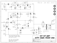
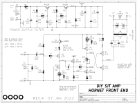
Two of the interchangeable Ship Of Theseus front end cards use circuits which strongly resemble your Bastode. They are labeled "Rush Cascode" which may or may not be a perfect synonym for Bastode.
"Kitty Hawk" uses an N-ch JFET and PNP, while "Hornet" uses a P-ch JFET and NPN. The Hornet circuit also includes a degeneration resistor (R9) to adjust the tradeoff between slew rate and bandwidth.
Numerous diyAudio members have built these and they are very pleased with the sonic performance.
_
"Kitty Hawk" uses an N-ch JFET and PNP, while "Hornet" uses a P-ch JFET and NPN. The Hornet circuit also includes a degeneration resistor (R9) to adjust the tradeoff between slew rate and bandwidth.
Numerous diyAudio members have built these and they are very pleased with the sonic performance.
_
Attachments
I follow this formula, the (internal) source resistances are in series, so that accounts for the reciprocal transconductance too....as they are connected in series, the composite gm1 will follow: 1/gm1 = 1/gmQ1 + 1/gmQ2
because transconductance is just the reciprocal of output resistance seen from the drain.
"... of output resistance seen from the drain." is another odd one: which output resistance? The (internal) source resistances or the drain output resistance? 'Seen' from the drain...
From this article:an equation handy for determining the BJT gm under a given collector current
For a given DC collector curremt ( Ic ) the slope of the function Ic = Is * exp(Vbe/Vt) is:
gm = d(Ic)/d(Vbe) = 1/Vt * Ie * exp(Vbe/Vt) = Ic/Vt
Notice the typos 'curremt' and the change from "Is" to "Ie"
But resumed & rewritten anyhow:
Ic = Is * ( e^[Vbe/Vt] - 1) (#10, Is = Icob)
d(Ic) / d(Vbe) = ( 1 / Vt) * Is * ( e^[Vbe/Vt] - 1)
The natural exponent has the nasty quality to reappear after differentiation (not to disappear), only the power comes forward.
So the last part of the equation... "= Ic/Vt" should be understand better when written:
gm = ( 1 / Vt) * Ic => gm = Ic / Vt
I've always (>> 40 years) only seen this equation as (the internal emitter resistance) re = Vt / Ic.
And 1 / re = gm indeed...
Nice lecture.Early effect is the phenomenon of BJT where the Ic-Vce curve reversely extends and crosses the x axis at a certain voltage (called Early voltage), so the output resistance of a BJT can be modeled as a resistor whose current rises by Ic when given a voltage VA across.
The 'certain voltage' is negative, so in equations better noted as |Ve| to avoid errors.
The phrase "...the output resistance of a BJT can be modeled as a resistor whose current rises by Ic when given a voltage VA across..." is confusing: a resistor whose current rises ?
This one (taken from the link):

is assuming that VA is much larger then Vce, while two inch (on my screen) above:

... so VA (Vearly) is not that much larger then Vce. It will be larger in most cases, equal sometimes or even lower (rare).
But to wipe it from the equation is another firm step.
Is it possible te rewrite your initial equation (#1) with all issues discussed above from formal to boiled-down so everybody benefits & can participate further discussions about this circuit?
ps:
I remembered this from long ago suddenly: Gm = 40 * Ic -> A = Rc / re = Gm * Rc = ( Rc * Ic ) / Vt ... not used this one for decades.
Source, source! Nevermind my brain will sometimes bug.which output resistance? The (internal) source resistances or the drain output resistance?
Well, for the batch of BC547 I used, I measured their Early voltage (VA) to be 120~150V. Also the value is not really fixed because I had a batch of BC547 from another manufacturer with VA near 100V. The Vce in my application will be 12V, so yes, to be precise the output resistance should be (VA+Vce)/Ic, but for all practical purposes I just use VA/Ic irl.But to wipe it from the equation is another firm step.
Last edited:
And thanks Mark Johnson for the insight. That's what I've been looking for! Unfortunately I couldn't use a NJET+PNP combo because my FETs have too high threshold voltage (and the BJT takes too much bias current for my application... maybe a Darlington will be better). But glad to see that there are some practices for such an architecture.
Wow no one has mentioned the bad bad setup with one J-Fet & And One Mosfet In A bastode configuration,,, witch is more or less the exact same topology as an differential amp, minus CCs, and the most imortant thing in thd & offset in regard to diff amps is to get matched transistors to minimize distortion and drift...... and here we have a bastode with devises of completely different types with probably wildly differing fro 10:1 Too 100:1 in transconductance,, witch borders for much distortion and so on..... a bastode is basicly a vertical diferetial amp,,, with much of the same criterias and needs for matching and so on,,, at least if the tought is that it should come near hi fi.......
Bests Of Regards To All Hi-Fi Lovers...... 🙂
Bests Of Regards To All Hi-Fi Lovers...... 🙂
Last edited:
Iraka... 🙂
have you meusured distortion in regard nto using two identical devices in the bastode section, versus you setup with not only different transistors,, but also different transistor thecnologys.??????
And if so how much distortion and how much difference from yours and my sgestion to use to identical matced devices as one usually do in diff Amps.....
bests Audiomaestro from Viking NORWAY
If fets has to high Vgs for bastode,,, then make it diff with ccs and it dont matter at ALL!!
best from NORWAY
best from NORWAY
very cool Anyways,,
Allthoug some of my audio (( Besides RF Anplifiers wich i nalso build since i am an RadioAmature )) design rules entails to always cascode gain Stages & large volt swinging stages,, so as to keep if possible both voltage & Current reasnable steady in the gain device.. And always running burning hot CLASS-A, Preferably several times the signal Current..., And Also important Only One Or max twoo gain stages in a whole audio chain,, and if two stages they need to run @ the same currents & voltage swing so as to UNDU As Much of the first Stage's distortion As Possible.......
Best Of regards.....
May We All Get To Hi-Fi ValHalla.... 🙂
Thanks for your feedback! To be honest this is just a proof-of-concept and simplistic design for DIY, and I don't expect such a circuit with only 4 transistors to be able to reach the performance of a circuit with 20 transistors. I designed it to be as simple as possible for testing, and if I were to build something for hi-fi I certainly would choose the LTP and CCS route. Or just use a dedicated opamp if unwilling to bother.Wow no one has mentioned the bad bad setup with one J-Fet & And One Mosfet In A bastode configuration,,, witch is more or less the exact same topology as an differential amp, minus CCs, and the most imortant thing in thd & offset in regard to diff amps is to get matched transistors to minimize distortion and drift...... and here we have a bastode with devises of completely different types with probably wildly differing fro 10:1 Too 100:1 in transconductance,, witch borders for much distortion and so on..... a bastode is basicly a vertical diferetial amp,,, with much of the same criterias and needs for matching and so on,,, at least if the tought is that it should come near hi fi.......
Bests Of Regards To All Hi-Fi Lovers...... 🙂
Of course this circuit can also be improved by adding cascodes here and there, and inserting buffers between the stages and at the output. But I think there's no point of doing so because the conventional three-stage design is well documented and certainly better than using Bastode alone.
- Home
- Amplifiers
- Solid State
- FET Bastode Input Stage Experiment