AndrewT said:Hi GK,
why did you choose not to insert an EF buffer between the q10 cascode and the driver pair?
All else looks much as you would be expected to produce.
Excellent front end to a power amp?
Hi
I take it you mean as in a triple EF? I didn't do it because there isn't any benefit with a 500 ohm load - the loading of the VAS is extremely light. Look at the loop gain plot at 1Hz - about 140dB of gain.
Cheers,
Glen
Hi,
In support of the ZFC ((c) Bonsai ;-), here an experimental diamond buffer with a fet frontend.
Part count (and complexity) is slightly higher, and of course a Zout of ~11Ohm. But that often doesn't matter much...
Cheers, Klaus
In support of the ZFC ((c) Bonsai ;-), here an experimental diamond buffer with a fet frontend.
Code:
THD 20kHz @ 7Vrms into 500R : 0.000027%
THD 20kHz @ 1Vrms into 500R : 0.000001%
THD  1kHz @ 1Vrms into 500R : 0.000001%
Part count (and complexity) is slightly higher, and of course a Zout of ~11Ohm. But that often doesn't matter much...
Cheers, Klaus
Attachments
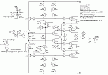
Here, ~12Vp (8.5Vrms). It strongly depends on the choosen cascode voltage, here ~10V. If I reduce it to ~5V, I can get 20Vp into 1k, with THD20 = 0.000123%. Load does the most to the THD figure. It's a brute force class-heat design, after all, so when the outputs see much current swing things start to get bad soon. The cascoding is the main trick to get those insane simmed (ahem) THD numbers, but there are some stablilty issues, also offset will probably need active control if it's to be used as a standalone buffer.
- Klaus
- Klaus
KSTR said:In support of the ZFC ((c) Bonsai ;-), here an experimental diamond buffer with a fet frontend.
Some major bootstrapping going on there! Love the floating current source too
") .
.no, I was thinking about the high output impedance of the cascode feeding the double EF stage.G.Kleinschmidt said:I take it you mean as in a triple EF? I didn't do it because there isn't any benefit with a 500 ohm load - the loading of the VAS is extremely light.
A simple follower presents a low source impedance to the output stage and I'm told the output stage returns a reward to the designer who does this.
But maybe, as you point out, that the loading is so low the drivers don't mind too much.
AndrewT said:no, I was thinking about the high output impedance of the cascode feeding the double EF stage.
A simple follower presents a low source impedance to the output stage and I'm told the output stage returns a reward to the designer who does this.
But maybe, as you point out, that the loading is so low the drivers don't mind too much.
OK. But, the HF the output impedance of the VAS is very low due to the nfb around it incurred by the miller comp.
KSTR said:Here, ~12Vp (8.5Vrms). It strongly depends on the choosen cascode voltage, here ~10V. If I reduce it to ~5V, I can get 20Vp into 1k, with THD20 = 0.000123%. Load does the most to the THD figure. It's a brute force class-heat design, after all, so when the outputs see much current swing things start to get bad soon. The cascoding is the main trick to get those insane simmed (ahem) THD numbers, but there are some stablilty issues, also offset will probably need active control if it's to be used as a standalone buffer.
- Klaus
Hmmmm.....
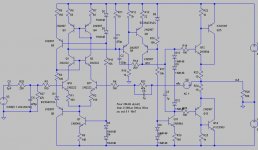
Very nice, but I'm not sure that I would call that a ZFC design, and your THD figures were not that hard to beat. A few tweaks to the OPS, bjt's in the LTP and a miller comp change to compensate for the extra gain of the LTP. I have a 65 deg phase margin, so stability isn't much of a concern and I am running a reasonably modest OPS bias current of 30mA. Offset voltage is negligible as input bias current is temperature compensated (see R21). Z-out is next to nill.
THD-20, 7Vrms into 500 ohms:
Code:
Harmonic  Freq	   Fourier 	Normalized
 Number   [Hz]     Component	 Component
    1   2.000e+04  9.956e+00	1.000e+00
    2   4.000e+04  2.176e-06	2.186e-07
    3   6.000e+04  6.110e-07	6.137e-08
    4   8.000e+04  1.775e-07	1.783e-08
    5   1.000e+05  5.236e-08	5.259e-09
    6   1.200e+05  1.561e-08	1.567e-09
    7   1.400e+05  1.443e-08	1.450e-09
    8   1.600e+05  2.105e-08	2.114e-09
    9   1.800e+05  2.286e-08	2.296e-09

Total Harmonic Distortion: 0.000023%
Cheers,
Glen
Attachments
CCS stolen from one of Edmond's designs...
I wouldn't worry about it; it wasn't really novel when Edmond did it either.
Linked proof producible on request.
Hi Glen,
I agree that it is arguable wether my buffer is zero global feedback or not, as there are two backward paths (if one takes this as a very strict GFB criterion). One might classify these linearizing bootstrappings as "indirect signal feedback", but at least there is no conventional global feedback along the lines of reducing some high open-loop gain, because the is no voltage gain stage present. Local feedback is of course found at various places.
I'd say your circuit is the winner here: less complex, controlled offset / Q-points, low Z-out (but, ahem, did you check PSRR? R11/C1 might be a pitfall -- probably better hooked to GND, assuming there is a clean GND). The impedance matching looks fine, still one could tweak to be fully AC balanced.
So we have now two circuits which seem to play in the same league of basic specs (assuming some real world relevance of the sim's)... now some "golden ear" might build them, refine both to perfection and then tell us if the GFB-design "sucks out the life of the music". I personally don't think so...
- Klaus
Feedback and high-order distortion spectra
I've put up a couple of posts on the permanent negative feedback thread showing some data on the effect of negative feedback on the creation and/or exacerbation of high-order distortion spectra.
In the first post I show data from actual power amplifiers gleaned from Stereophile reviews. This data is the odd-order 19 & 20 kHz CCIF distortion spectra that lies in-band from 18 kHz on down. Data is shown for odd-order distortion out to 9th order. The data is for a group of power amplifiers including no-feedback through high-feedback designs.
The other posts show distortion simulation data for a single-stage CE BJT amplifier. Graphs of THD out to 7th order are shown for:
1) The CE amplifier with no emitter degeneration with varying amounts of global NFB;
2) The CE amp with varying amounts of emitter degeneration but with no global NFB;
3) Then finally with a fixed amount of emitter degeneration and varying amounts of global NFB.
Cheers,
Bob
KSTR said:Hi,
In support of the ZFC ((c) Bonsai ;-), here an experimental diamond buffer with a fet frontend.
Code:THD 20kHz @ 7Vrms into 500R : 0.000027% THD 20kHz @ 1Vrms into 500R : 0.000001% THD 1kHz @ 1Vrms into 500R : 0.000001%
Part count (and complexity) is slightly higher, and of course a Zout of ~11Ohm. But that often doesn't matter much...
Cheers, Klaus
Hi Klaus,
cool you working that further! While I'm not sure, if the huckepack-current mirror is really necessary, I like the fact you try to promote the weird cascode (Q1/Q2 to the outout Q's).
Rüdiger
KSTR said:Hi Glen,
I agree that it is arguable wether my buffer is zero global feedback or not, as there are two backward paths (if one takes this as a very strict GFB criterion). One might classify these linearizing bootstrappings as "indirect signal feedback", but at least there is no conventional global feedback along the lines of reducing some high open-loop gain, because the is no voltage gain stage present. Local feedback is of course found at various places.
I'd say your circuit is the winner here: less complex, controlled offset / Q-points, low Z-out (but, ahem, did you check PSRR? R11/C1 might be a pitfall -- probably better hooked to GND, assuming there is a clean GND). The impedance matching looks fine, still one could tweak to be fully AC balanced.
So we have now two circuits which seem to play in the same league of basic specs (assuming some real world relevance of the sim's)... now some "golden ear" might build them, refine both to perfection and then tell us if the GFB-design "sucks out the life of the music". I personally don't think so...
- Klaus
Hi Klaus.
R11/C1 don't actually have any effect on the PSRR and referencing the network to gound is the worst thing that you can do with it. R11/C1 simply shunts the input to the VAS, which is referenced to the positive supply rail anyway.
It is C2 (miller comp) which has the greatest effect on PSRR, as in any miller compensated amp, so a real world version would need some filtering of the rails - but even a simple RC can make the PSRR of a miller compensated VAS (expecially throughout the audio range) extremely high.
Cheers,
Glen
Hi Rüdiger,Onvinyl said:Hi Klaus,
cool you working that further! While I'm not sure, if the huckepack-current mirror is really necessary, I like the fact you try to promote the weird cascode (Q1/Q2 to the outout Q's).
Rüdiger
the complex CCS/mirror stuff is only there to get an excellent PSRR, although it also affects linearity performance a bit. Basically, simple LED-type CCSs would do it as well.
To be useful and proven-good in reality, that circuit in general will certainly need a lot of refinement and even simplification.
- Klaus
KSTR said:Hi Glen,
I don't see any basic difference in which AC GND one chooses to connect that network. If it is GND though, then there is another cap in series and maybe some stray inductance too, so this might be more critical indeed.
- Klaus
OK. AC GND is AC GND, but the PSRR would be compromised by connecting the aditional RC network to GND instead of the positive supply rail. The input the the VAS is referenced to the positive supply rail. If the RC was connected from the VAS input to GND instead of from the VAS input to the positive supply rail, voltage fluctuations on the positive supply rail (WRT GND) will induce an AC current through the RC; therefore modulating the VAS.
Cheers,
Glen
- Status
- This old topic is closed. If you want to reopen this topic, contact a moderator using the "Report Post" button.
- Home
- Amplifiers
- Solid State
- Feedback Question/Clarification