I tried lots of adjustments of the "Zen pots" (the pots across the source resistors), but I was troubled by not being able to find a subset of 4 out of 6 R100s that would provide 2 channels that could be adjusted similarly.Lhquam,
May I ask you....
Did you really play with the k2/k3 ratio at the normal F6?
Did you hear F6 for instance k3 dominant like your F5?
Sorry when you wrote it already in a post.....")
When I was doing those tests I did not fully understand how to control both H2 and H3. The Zen pots affect both H2 and H3, and H3 is minimized by adjusting the Zen pots to the source end. H2 is minimized by balancing the open-loop gains to the upper and lower halves of the push-pull amplifier. This is easily accomplished by adding one or more pots across the transformer secondaries, with the wipers attached to the gate-stopper resistor. That is what I am doing in the F6CC.
BTW: The F6CC PCB it trivially modified for use without output FET cascoding by jumpering source to drain on pads for the cascode FETs. Thus we get a complementary FET version of the F6.
I have them on 25V rails. 1A bias is most i can go comfortably for long term with current sinks. My new toroid will give me 22V rails, so bias will be increased to 1.2A. I am thinking i have about 60W class A at that point. If i can get a free moment, I will start posting some measurements.
Quick question. Major OT for cascode man What happens if you place a resistor in between the cascode device and the protected device? Also, what if we put a pot acrss the Jfet Rs, with output attached to cascode device through cap. We have similar adjustablilty to that of output of F6, correct.
Quick question. Major OT for cascode man
What happens if you place a resistor in between the cascode device and the protected device? Also, what if we put a pot acrss the Jfet Rs, with output attached to cascode device through cap. We have similar adjustablilty to that of output of F6, correct.I have them on 25V rails. 1A bias is most i can go comfortably for long term with current sinks. My new toroid will give me 22V rails, so bias will be increased to 1.2A. I am thinking i have about 60W class A at that point. If i can get a free moment, I will start posting some measurements.
Quick question. Major OT for cascode man
I am considering attaching my 7" x 10.8" heatsinks fin-to-fin with a pair of low noise PC fans. If the power requirements are low enough, convective air flow will work, otherwise crank up the fan speed. Another advantage of this is that the PC boards are more accessible, being on the outside of the heatsinks rather than the inside.
Putting a resistor of value R between them will decrease the effectiveness of cascoding, since as the current thru the FETs increases, the Vds of the drive FET will decrease by the amount I*(1/Gm+R), where Gm is the transconductance of the cascode FET. The variation of Vds is minimized by making R=0, or negative. It would be great if R=-1/Gm
. Hint: Cascode modulation in Zen Variation #9. I need to try that in F6CC. Thanks for reminding me about that.
Last edited:
I wouldn't call it degeneration of the cascode. Usually degeneration refers to reducing the gain of a common-source stage by adding a source resistor, and "linearizing" its operation. Unfortunately, it also creates local feedback and higher order harmonics. I will produce a concept drawing as applied to the F6CC. In the meantime study Cascode Modulation in Zen Variations 9[FONT=Arial, sans-serif]. [/FONT][FONT=Arial, sans-serif][FONT=Arial, sans-serif]http://firstwatt.com/pdf/art_zv9.pdf. [/FONT]It might be explained differently there, but the idea is to negate the [/FONT][FONT=Arial, sans-serif]effect of the variation in Vgs of the cascode FET due to change in current by using the drop across a source resistor on the output drive FET. In the F6 and F6CC, that source resistor does not necessarily create AC degeneration of the drive FET. [/FONT]Is this a way to degenerate the cascode? What about pot across the Rs of the Jfet, attached to base/gate of cascode, allowing tweaking like in F6 output?
Oops, I didn't think that last one through. Zen Variations 9 isn't the answer. The sign on the cascode modulation is wrong for what I wanted.
What you say
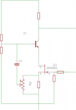
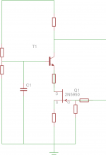
 first or second drawing. Da^n, I am confusing myself.
That is what I was thinking, but the increasing the pot toward the rail increases the Vds variation of Q1. In ZV9, Nelson found a "Sweet Spot" where that was beneficial, but I have no hope for such a sweet spot with the MOSFETs I am using. With a balanced amplifier, it would be easy to obtain a modulation voltage with the opposite sign.This is the first and second item I was referencing, in wrong order.
Mind drawing it. I am thinking of the above for the input of an F5 like circuit.
Attachments
I am not sure it works. I need to quit "shooting from the hip" and run some sims before putting out designs.I just like it.

Still the wrong polarity of modulation.I think someone did simliar configuration with the F5 where the crossing took place at the bjt cascodes on the FE vs at the ource pins of the input pair. I do not see why it would not work, as they are looking at a low Z point on the opposing fet.
- Home
- Amplifiers
- Pass Labs
- F6 Amplifier