Can anybody help me about this;
http://www.diyaudio.com/forums/power-supplies/302072-power-supply-jlh2003-f5-amplifier.html
http://www.diyaudio.com/forums/power-supplies/302072-power-supply-jlh2003-f5-amplifier.html
Hello,
do you guys think this chassis is ok for a F5.
https://www.aliexpress.com/item/Cla.../1889983188.html?spm=2114.13010308.0.0.2eagV3
Thanks
do you guys think this chassis is ok for a F5.
https://www.aliexpress.com/item/Cla.../1889983188.html?spm=2114.13010308.0.0.2eagV3
Thanks
Hello,
do you guys think this chassis is ok for a F5.
https://www.aliexpress.com/item/Cla.../1889983188.html?spm=2114.13010308.0.0.2eagV3
Thanks
I think this one is a better deal.
Dissipante 4U – diyAudio Store
Rush
Thanks. I'm just afraid of duty and shipping costs. but indeed that dissipante 4U is a very good deal.
Hi everybody,
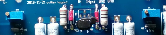
I'm about to power up my F5 and am getting a little nervous. I know I am betraying my ignorance here and I'm sure this has been addressed somewhere here but I would just like confirmation that P1 and P2 should set to 0(zero) ohms resistance. I set resistance to zero ohms between #1 and #2 pins on the trim pots before soldering. That meant, with the adjustment screw to the left, the screw turned all the counter clockwise. Just want to confirm that is correct. Attaching a photo of my board. I'm still learning so I guess I don't understand how biasing actually works: how do you get more voltage by increasing the trim pot resistance? My AC and DC voltage were fine, tested with dim light bulb. I bought a Variac for first startup. Is there anything I need to keep in mind while using the Variac? I would really appreciate any advice.
Thanks
Attachments
Make sure you have 3 volt meters on the board. Turn the pots 3 turns at a time, one after another until you see bias voltage. You will notice that P1 increases DC offset and P2 decreases it. You have to "walk" the bias voltages up one at a time while dialing in the offset at the same time. If it gets weird or one pot is turned all the way out, go back to zero ohms and start over. You'll get the hang of it.
The jFETs draw a nearly constant current, maybe around 8mA.............I would just like confirmation that P1 and P2 should set to 0(zero) ohms resistance. I set resistance to zero ohms between #1 and #2 pins on the trim pots before soldering. .....................I don't understand how biasing actually works: how do you get more voltage by increasing the trim pot resistance?......................
The resistors and the parallel pot act as drain loads.
If the resistance of the Drain load is set to 0ohms, then the Vdrop will be 0V
This voltage is applied across the output mosFET gate to source.
Now turn the pot up a bit.
It is now @ 100r and the other resistors in parallel give ~95r of total Drain load resistance. With 8mA flowing through 95r you get a Vdrop of 0.76V
This is too low to turn on the output mosFET.
You keep turning the two pots until the mosFETs start to turn ON. This needs ~2.5V to 4V. The pots need to be turned up (maybe around 500r) to give this turn ON Vgs. To get to your final HOT bias current the pots might end up around 1000r, but they will be different. Because the Vgs of the upper and lower mosFETs are different. They need a different Vgs to pass the same current. It is this SAME current that results in zero output offset.
That's why the pot resistances need to be increased to get the outputs to pass current.
Last edited:
Hello Guys .
I'm about to start to assembly my F5 and order of components.
I'd like to confirm that for the V3 of the pcb R3 and R4 should be 10 ohms and what is the power rating for it? 1/4 w?
Another question is how accurate is the V3 schematic that is available on the diystore?
F-5 – diyAudio Store
F5 is my first class A amp... I want to avoid any re-works on the PCB as much as possible.
Thanks in advance.
R3 and R4 should be minimum 1/2W, preferably 1W. At 20V output these dissipate close to 1.2W peak so a 1/4W part is pushing it specially if you listen/need to listen loud.
thanks
R3 & 4 are in series with the 50r NFB resistors.Hello Guys .
I'm about to start to assembly my F5 and order of components.
I'd like to confirm that for the V3 of the pcb R3 and R4 should be 10 ohms and what is the power rating for it? 1/4 w?
Another question is how accurate is the V3 schematic that is available on the diystore?
F-5 – diyAudio Store
F5 is my first class A amp... I want to avoid any re-works on the PCB as much as possible.
Thanks in advance.
The current through these is ~ Vpk/(50+10) = 30Vpk/60 = 0.5Apk.
The peak instantaneous dissipation will be 0.5Apk² * 10ohms = 2.5W
the average will be half of this if the output stays that high for long enough and the duty cycle is 50% so the average dissipation if testing with sinewave to 30Vpk (56W into 8r0) would be 0.625W
That is too much for a 600mW resistor.
But there is a recommendation (by a few) that the NFB resistor/s should not be exposed to dissipations exceeding 10% of their rating.
Ordinary VFA amplifiers can meet this requirement fairly easily. Not CFA and not the F5.
R3 & 4 are in series with the 50r NFB resistors.
The current through these is ~ Vpk/(50+10) = 30Vpk/60 = 0.5Apk.
The peak instantaneous dissipation will be 0.5Apk² * 10ohms = 2.5W
the average will be half of this if the output stays that high for long enough and the duty cycle is 50% so the average dissipation if testing with sinewave to 30Vpk (56W into 8r0) would be 0.625W
That is too much for a 600mW resistor.
But there is a recommendation (by a few) that the NFB resistor/s should not be exposed to dissipations exceeding 10% of their rating.
Ordinary VFA amplifiers can meet this requirement fairly easily. Not CFA and not the F5.
So are you saying that R3 and R4 should be 30w? or the peak dissipation shouldn't exceed 110% of it rating.. and than 3W should be ok.?
Thanks
R3 and R4 should be minimum 1/2W, preferably 1W. At 20V output these dissipate close to 1.2W peak so a 1/4W part is pushing it specially if you listen/need to listen loud.
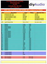
I'm using 10R 1W for R3 and R4 per attached F5 v3 BOM. I'm using the schematic from Nelson's F5 Turbo article. It's the first one in the article, "...official DIY F5 schematic". I hope those two are correct.
Attachments
Try checking the temperature of the feedback resistors while testing the amplifier to nearly clipping, without any load connected.
As I said it is fairly easy with a VFA amplifier to keep the feedback resistor temperature pretty low. They feel cold to the touch.
That does not apply here.
As I said it is fairly easy with a VFA amplifier to keep the feedback resistor temperature pretty low. They feel cold to the touch.
That does not apply here.
Last edited:
It's the output voltage that determines the current through the feedback resistors.Also lower is the speaker resistance on the output it will make much less current to go thru those resistors.
Pass gave us a good clue when for the F5 he specified a pair of big resistors for the upper leg.
- Home
- Amplifiers
- Pass Labs
- F5 power amplifier