Has anyone here Successfully used this P3 in a F-5, and if so, what were your sonic observations in utilizing it? I'm curious! But the only reports I've seen were from B. sabth who didnt have much luck, I dont want to fry any of my Jfets if possible! Thanks!
Russellc
seems some equipment and understanding is essential
Russellc
P3 in R1 schematic have same purpose as additional source resistor( of output mosfet) on one side - which you can see on any original FW F5 picture .
fine fiddle with signal gene + THD meter is needed for setting .
what's important is knowing that you must be careful , approaching extremes of that pot
seems some equipment and understanding is essential
Hi Russellc
Glad that at least that bit of smoke helped someone not to make more smoke
I have not given up Just postponed.
(I need beter gear before the F5 to make a better F5)
Tanks buzzforb (of course silly me) go to get back and read the tread but cant remember
the argument about detrimentall efects on cascoding an F5
Hi
Just wanted to share my build so far.
Also would like some constructive criticism.
First impressions are very good in my system compared to my 845set. I noticed pretty much all the things other builders have described in previous posts. Highs are more detailed, bass is fast and tight. All good.
In the attached photos are the temperatures I've measured, i feel the mosfets (Fairchilds running at 1.4A) are running a bit cool due to the big heat sinks(conrad 151 x 350), as somebody told me these sound better at 100 degrees C.
The diodes I'm using are BYV29. As you can see they are operating at 36 degrees C
Also in the photos you'll notice R4 has had the resistance increased quite a lot on one of the channels, i got up to about 9k! I know others have had to increase R4, what did they increase to? I guess its a matter of how far out the Vgs is on the p channel. Is it worth getting closer matched mosfets? Ive got some matched jfets on there way.
As you can see I'm using very standard wires. What are some examples of better wire which could be used in the various parts of the circuit? Probably invest in some shielded for input. Also layout will change once i get it into a home. Other suggestions?
This build is going to be a work in progress for some time to come. I'm really looking forward to experimenting in the power supply, different resistors, caps, etc.
What are some other parts people have changed over and noticed changes and improvements?
Any advice welcome.
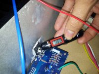
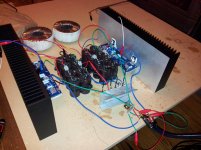
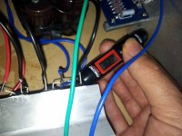


Last edited:
Hi ryan. Your build looks good so far. What grade of jfets to you get? You might find that it is easier to get the vgs up high enough when you have higher idss jfets. Regarding the temp, I don't think you should worry about running them too cold. When you assemble the chassis, your heat sinks will lose a lot of efficiency.
I am making an F5 (with multiple output devices) in little steps.
1)
2) test the jFETS, and group them (match is a big word), I selected a 10 mA K170 and a 12 mA J74; I soldered them in the board (only input stage):
- There is a difference in gain of 10 dB [/B] between the two halves with a 2SK170/2SJ74 attached to a about 230 ohm drain resistor; and just for certainty I connected a 2SJ74 of 20 mA - and that gave a difference of almost 13 dB.
albert
UPDATE and WARNING

I have recieved a new batch of FETS from new supplier. These new ones are OK. I will post separately on those.
The 2SJ74's I bought from my first supplier are FAKES. That is why they do not match the 2SK170's in any way.
Some pictures:
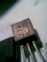
You can see the scratches from the sandpaper they used to get the original FET name off. The new name is 'melted' (a hot die) into the transistor.
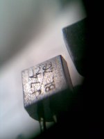
Here you see the faint original number 1271 on it. Wonder what FET this actually is (at 20 mA Idss) and rather low transconductance.
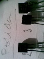
Here you can see the name of the supplier who is to go here:
 .
.oh well . . .
albert
Last edited:
... i feel the mosfets (Fairchilds running at 1.4A) are running a bit cool ...
That's not cool at all - look at the datasheet (thermal resistance between semiconductor and the case) and you'll see that the silicone inside your MOSFETs is well over 100 degrees Cels.
If you push the temp. on the MOSFET's case to 100 C you'll be very close to destroying them...
Thanks juma,
Can anyone advise on a safe max temp on the junction?
If im getting 76 C on the case (front) does this equate to about 88 C on the junction, if im reading the data sheet correctly?
Or is the "case" the back of the mosfet?
If so i guess i cant really measure that effectively.
Can anyone advise on a safe max temp on the junction?
If im getting 76 C on the case (front) does this equate to about 88 C on the junction, if im reading the data sheet correctly?
Or is the "case" the back of the mosfet?
If so i guess i cant really measure that effectively.
Last edited:
Make life difficult for the supplier.
Report the supplier. Did you find him/her through Ebay or similar?
Did you pay through PayPal or similar.
Make a claim through your credit card company for fraud.
I have opened a case in Paypal to reclaim the money. See what happens. Does PP send claim information to ebay?
albert
How do you make a power supply for the F5 ?
I am a bit lost here.
You're not lost, you just havent read the manual on the Firstwatt site. I think its about the last page.
Russellc
- Home
- Amplifiers
- Pass Labs
- F5 power amplifier