Good thing that mr Pass think different
Do you better skilled not need the help of Nelson just as much as we may need yours
Or is that different
I am not sure what you are saying?
Hello Juma and others
I made the PC board layout after your drawing . I just finished now .
Only question I have the 22uF caps are not to much ?
I did look up many design use cascode , designer usually use 1uF foil caps .
Also designer sometimes use Zener diode instead the resistor which goes to the ground ?
I see you are a experienced guy so I take your advise !
Also I sow cascoding the same way than Thanh tested only they use JET insted lateral or BJT .
I will each both version PC board design after your advise and the original design by Thanh .
I will see wich one will work .
I understand you say that is not is how work , but what about the design what you drawn that is bad also ??
I'm not interested on the original F5 , not because is not a great amp because I have the large heat sink , high power transformer and I have a dozen Toshiba mosfet .
Greets
Thanh, you have been very helpful, fore a very long time now
I like your good spirit and positive thinking, thanks
Juma also brought some light to things, thanks
garbobela, Im not sure you can expect it to work just like that, not wise to rush into it when yo dont know how to handle it
That was said by Thanh a few posts back, and I beleive Jumo backed out fore the same reason
He showed how it might work, but didnt say it would
It would ofcourse be very good if YOU can make it work, with some help, but that could appear a bit risky
And further, we cant be sure that it really works, even if you report back postively
Last edited:
Yes, but 36V is quite a bit more than 30V and that pushes the limit already. You can blame only your self when your JFET dies.It was stated clearly just few posts back, that 30V would work without cascode, and a few exstra outputs, but not higher than 30V(22V trafo)
There are amps around too running healthy on that
Not at all. It's just that Toshiba MOSFETs are considered a better choice.But now there seems to be issue with orginal IR outputs as well
I gave you schematic for cascoding of input JFETs that works quite well. What more do you want?And cascode not going well either
Not going well
No, but you are free to use whatever you want. Think a little why is that specific sub-circuit called "grounded Base"Only question I have the 22uF caps are not to much ?
Well, you'll have to learn more in order to be able to distinguish a working circuit from faulty one.I understand you say that is not is how work , but what about the design what you drawn that is bad also ??
Hi gaborbela
With that attitude gaborbela, you will learn a lot.
I will also learn to.
Jumas version is guaranteed to work, mine is not, but if it does work then this will be very valuable information, as it makes constructing easier.
Yes I would probably use Zeners too.
What bipolar are you going for?
Just be careful with TO-92, for some reason that I don't understand completely. The voltage drop across the cascode device and the JFET is not always equal.
Eg If you have 40V rails, then you don't necessarily get 20V across cascode and 20V across Jfet, it could be 30V across cascode and 10V across JFET.
I am not sure why but it seems to vary depending on the device.
What I am trying to say is, that the power dissipation does not necessarily get shared equally.
Last edited:
About transistor position
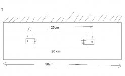
Hi.I have a look at the diyers pcbs and see that the distance between two transistors are short..I have 50cms long and 10 cms height 1,5kilograms cooler..have a look at the picture.Am i wrong?I remember that Nelson said far from eachother is better for good cooling.but most people does opposite of this.Why ?
Hi.I have a look at the diyers pcbs and see that the distance between two transistors are short..I have 50cms long and 10 cms height 1,5kilograms cooler..have a look at the picture.Am i wrong?I remember that Nelson said far from eachother is better for good cooling.but most people does opposite of this.Why ?
Attachments
juma Well said:Yes you right , but I do not need to understand everything how works to do or build something .
We can take advice from each-other .That is how we learn .
Otherwise we can start to learn from basic how a transistor work or purpose of resistors , capacitors etc . We would probably never arrive there to build something .
I really appreciate your advise and help !!!!!!
I read you wrote what you drawn that works , I will build it !
Thank you
The voltage sharing between gain and cascode device in this case depends only on DC Voltage on the BJT's base and it will be half of the +V (since we use two equal resistors - 4k7). The gain device will have 17.3V on the drain (36V / 2 - Vbe)....
Eg If you have 40V rails, then you don't necessarily get 20V across cascode and 20V across Jfet, it could be 30V across cascode and 10V across JFET.
I am not sure why but it seems to vary depending on the device....
Hi.I have a look at the diyers pcbs and see that the distance between two transistors are short..I have 50cms long and 10 cms height 1,5kilograms cooler..have a look at the picture.Am i wrong?I remember that Nelson said far from eachother is better for good cooling.but most people does opposite of this.Why ?
Ahh. . .the only thing I can think of is cost. I hope when and if someone does a J2 board they'll move those expensive output devices a little farther apart.
Hi Thanh
I built several amplifier at the last 20 years .
I'm willing to learn , and in the real life we faster than just reading books .Of course I take the advise of experts .
Books are great , I'm not against them but to build a amplifier I do not want to go to school or study weeks and months .
I look some example where the rail voltage it was 56V 1.5k resistor after BC550C/560C and 2SK170 /2SJ74 JETs.
I go with BC BJT-s , I will try to set up the bias slowly .If the cascode devise will get to hot probably after I try transistor in case TO220 .
Thank for your encouragement .
Greets
Not at all. It's just that Toshiba MOSFETs are considered a better choice.
I gave you schematic for cascoding of input JFETs that works quite well. What more do you want?
Regarding output, its another debate going on, about Faichilds being better but maybe selling relabelled IR, or at least thats how I understood it
Regarding your nice BC### cascode
Sorry I have got it all wrong
Didnt know it was a ready to go
I did thank you fore bringing some light into this
Its really great if that will work
No need to check wit scope and such
Now I will be silent and follow with interest
Hi Thanh
I go with BC BJT-s , I will try to set up the bias slowly .If the cascode devise will get to hot probably after I try transistor in case TO220 .
Thank for your encouragement .
Greets
You probably won't have any issues, but it is good to provide a reasonable amount of safety margin.
Good luck.
Do you have access to a lab power supply?
Last edited:
I think it comes down to parasitics.
Longer track lengths = higher parasitics = more chance of creating instability.
I could be wrong though
That sounds more like SMD IC, or other unstable curcuits
To me, it seem like Nelson puts the Jfet well away from outputs, so I suppose theres no issue
I also believe to remember he said to keep input away from supply lines
And that the most common cause of instability is wrong interconnects
Obviously the input Jfets are somewhat sensitive
Maybe best keep noisy lines away from them
Yes I agree with that.
I thought he was referring to keeping the output devices away from each other, for better heat dissipation.
I didn't think he was referring to output and input devices away from each other.
Ahh, yes ofcourse, I responded to the mentioning of parasitics
Nelson does put outputs far from each other, but remember if looking at F5, theres only one pair
Thanh, ofcourse your right about it when we use multiple pairs, the individual outputs on each side should be kept fairly close together, but I suppose theres a sensible limit to that too
Nelson does put outputs far from each other, but remember if looking at F5, theres only one pair
Thanh, ofcourse your right about it when we use multiple pairs, the individual outputs on each side should be kept fairly close together, but I suppose theres a sensible limit to that too
Last edited:
Without compensation, the bandwidth is typically around
1 MegaHertz, and that means well done grounding and
shielding on inputs and outputs, and not much tolerance
for capacitive loads at very high frequencies.
Internal layout with regards to transistor placement is not
critical.

1 MegaHertz, and that means well done grounding and
shielding on inputs and outputs, and not much tolerance
for capacitive loads at very high frequencies.
Internal layout with regards to transistor placement is not
critical.
I made the poor assumption that Juma thoroughly checked his circuit.
I thought I better check it, before people started building it verbatim.
To put it simply, it does not work at all.
Do not build it.
Just to let you know i used bc560 and bc550.
Juma can you check that you haven't made a simple mistake somewhere.
I thought I better check it, before people started building it verbatim.
To put it simply, it does not work at all.
Do not build it.
Just to let you know i used bc560 and bc550.
Juma can you check that you haven't made a simple mistake somewhere.
Last edited:
- Home
- Amplifiers
- Pass Labs
- F5 power amplifier