Unless you have a 32R phone, there is not a lot to gain to go to 200mA.
With 15V rail it will stay to clip at 12V, and low distortion (<0.1%) up to about 10V.
That would be 300mA for 32R load, or 200mA for 50R load.
But your decision, as the sinks and the devices will cope.
And you can always change the bias and listen before deciding.
Otherwise, I personally like to put all heat generating devices on ONE heat sink rather than each one individually.
It make sure that they all track each other thermally, hence somewhat lower thermal drift.
But I have no proof that it does not work otherwise.
And I would also connect all the heat sinks to either Gnd or Case.
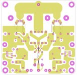
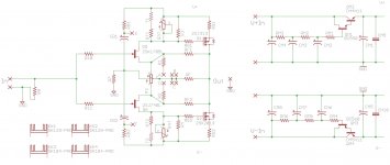
I do not quite understand why you do not use a flooding Gnd plan on top.
Even if you minimise stray capacitance, you only need to hollow out the few traces that carry signal.
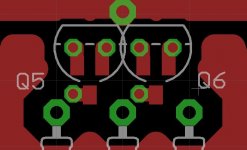
I also do not understand why you would not turn Q6 round 180° for fully symmetry.
If you want to keep the current configuration, I can tell you can the D & S pins of Toshiba JFETs are swappable.
And you may wish to make the output tracks much thicker, or the output connection much closer to the power Gnd return point.
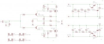
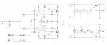
R1, R2, Rg1, Rg2 do not have to be power resistors.
And Rf1, Rf2 each will only dissipate a maximum of 25mW rms even if you are at maximum useful sinusoidal output (7Vrms) all the time.
And a separate Rf is not necessary. Two in parallel always have lower inductance.
One day when I am ready to release my own PCB (which is actually done), you will then see the difference.
Patrick
With 15V rail it will stay to clip at 12V, and low distortion (<0.1%) up to about 10V.
That would be 300mA for 32R load, or 200mA for 50R load.
But your decision, as the sinks and the devices will cope.
And you can always change the bias and listen before deciding.
Otherwise, I personally like to put all heat generating devices on ONE heat sink rather than each one individually.
It make sure that they all track each other thermally, hence somewhat lower thermal drift.
But I have no proof that it does not work otherwise.
And I would also connect all the heat sinks to either Gnd or Case.
I do not quite understand why you do not use a flooding Gnd plan on top.
Even if you minimise stray capacitance, you only need to hollow out the few traces that carry signal.
I also do not understand why you would not turn Q6 round 180° for fully symmetry.
If you want to keep the current configuration, I can tell you can the D & S pins of Toshiba JFETs are swappable.
And you may wish to make the output tracks much thicker, or the output connection much closer to the power Gnd return point.
R1, R2, Rg1, Rg2 do not have to be power resistors.
And Rf1, Rf2 each will only dissipate a maximum of 25mW rms even if you are at maximum useful sinusoidal output (7Vrms) all the time.
And a separate Rf is not necessary. Two in parallel always have lower inductance.
One day when I am ready to release my own PCB (which is actually done), you will then see the difference.
Patrick
Last edited:
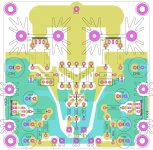
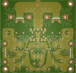
GND and OUT would be nice on same side if the board. Single sided even more nice. Lots of opportunity for pouring copper rather than traces have been overlooked. Jfets could be face to face. Power supplies easily rearranged to be closer to both input and output devices. Free some room by putting caps on opposite side of sinks unless you're worried about cap+heat. Holes for sinks have no copper. If you ever try to desolder one you'll pull off the small copper rings also. I like larger through hole pads anyway on everything. Makes things easier from the start. I would bet your large resistor holes are too small for leads. 1/4w should be .8-.9mm. Larger probably 1.4mm. Trimmer pads way too small. You'll cook trimmers.
My 2cents. Something nagging me about R7. (Patrick addressed it)
My 2cents. Something nagging me about R7. (Patrick addressed it)
Last edited:
Since there seems to be multiple people tempted to build, perhap it is time to mentioned some additional features, especially for beginners.
The original F5 power amplifier has some additional safety circuits to limit maximum current through the output devices.
This protects the amplifier in case of an output short circuit.
Although there are report that they do adversely affect sound quality, you might still want to add those in.
The idea is to measure the voltage across the 3.3R source resistors with a potential divider.
This in turn is used to switch on a BJT (when Vbe > 0.6V) that shunts the gate voltage to the power rails.
In doing so, the MOSFETs current is reduced to the set limit.
I'll leave it a an exercise for those who wish to include this.
There are very detailed explanations in both the F5, F5X and Aleph-X articles.
They all have the same protection circuit.
")
Patrick
The original F5 power amplifier has some additional safety circuits to limit maximum current through the output devices.
This protects the amplifier in case of an output short circuit.
Although there are report that they do adversely affect sound quality, you might still want to add those in.
The idea is to measure the voltage across the 3.3R source resistors with a potential divider.
This in turn is used to switch on a BJT (when Vbe > 0.6V) that shunts the gate voltage to the power rails.
In doing so, the MOSFETs current is reduced to the set limit.
I'll leave it a an exercise for those who wish to include this.
There are very detailed explanations in both the F5, F5X and Aleph-X articles.
They all have the same protection circuit.
Patrick
Patrick & Udailey, many thanks for your comments, I'll redo the board.
Remember that copper tracks has inductance.
That is not desirable for a high bandwidth circuit like the F5-HA.
So wide, short tracks are called for.
And that mean a compact layout as much as possible.
And thin film resistors are always better as long as they can take the dissipation.
Patrick
F5-HA builders should also read this, especially post #12~14.
http://www.diyaudio.com/forums/pass-labs/274872-problem-toasty-resistor-f-5-a.html
Patrick
http://www.diyaudio.com/forums/pass-labs/274872-problem-toasty-resistor-f-5-a.html
Patrick
0.65mm diameter holes are sufficient for 0.6mm diameter lead outs....................I like larger through hole pads anyway on everything. Makes things easier from the start. I would bet your large resistor holes are too small for leads. 1/4w should be .8-.9mm. Larger probably 1.4mm. Trimmer pads way too small. You'll cook trimmers.
My 2cents. Something nagging me about R7. (Patrick addressed it)
1.1mm diameter holes are sufficient for 1mm lead outs.
Last edited:
Andrew
RN55D have .64mm leads. HASL adds 10-15um on pads so double that in a hole and then HASl. Board houses dont drill what you spec. They drill their closest equivalent drill bit and then add a collar to the hole. If you actually spec what you need you will end up with useless boards. Once bitten twice shy.
RN55D have .64mm leads. HASL adds 10-15um on pads so double that in a hole and then HASl. Board houses dont drill what you spec. They drill their closest equivalent drill bit and then add a collar to the hole. If you actually spec what you need you will end up with useless boards. Once bitten twice shy.
then a 0.7mm and 0.75mm diameter hole will fit.Andrew
RN55D have .64mm leads.
Now you are showing that you know how to arrive at the correct hole diameter. Use this method instead of just jumping at a far too big hole.HASL adds 10-15um on pads so double that in a hole and then HASl. Board houses dont drill what you spec. They drill their closest equivalent drill bit and then add a collar to the hole. If you actually spec what you need you will end up with useless boards. .......
Discussion more appropriate in this thread ?
http://www.diyaudio.com/forums/parts/91101-pcb-hole-size.html
Thanks,
Patrick
http://www.diyaudio.com/forums/parts/91101-pcb-hole-size.html
Thanks,
Patrick
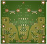
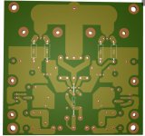
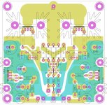
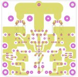
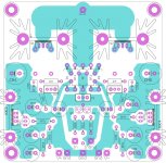
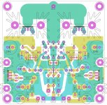
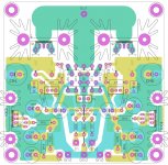
Next iteration:
- more signal polygons instead of traces
- enlarged some traces (output )
- enlarged pads and holes on many packages
- swapped jfet drain-source for symmetry
- added ground polygon on input
- added film caps placeholders C1,C2 parallel with multiplier output caps just in case
Open questions:
1. Ground pour on feedback network, fets, heatsink, output
2. Position of output ground
Regarding R7, not understand, R7 (optionally) connects feedback network to star ground, connection now separated from input ground, where is the problem?
Regarding Rf, 3 is better then 2 (lower inductance).
Regarding power resistors, not really important.
Grounding: all different grounds are connected on star, seems near ideal to me.
Regards, Sika
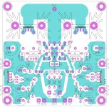
- more signal polygons instead of traces
- enlarged some traces (output
)- enlarged pads and holes on many packages
- swapped jfet drain-source for symmetry
- added ground polygon on input
- added film caps placeholders C1,C2 parallel with multiplier output caps just in case
Open questions:
1. Ground pour on feedback network, fets, heatsink, output
2. Position of output ground
Regarding R7, not understand, R7 (optionally) connects feedback network to star ground, connection now separated from input ground, where is the problem?
Regarding Rf, 3 is better then 2
(lower inductance).Regarding power resistors, not really important.
Grounding: all different grounds are connected on star, seems near ideal to me.
Regards, Sika
Attachments
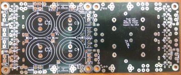
Companion DC board just arrived.
Attachments
Unless you have a SOT23 test socket, you cannot do matching properly.
So it is better to first solder onto an adaptor, match, before soldering onto PCB.
Also helps to get rid of heat better by gluing a small heat sink onto the adaptor.
http://www.diyaudio.com/forums/atta...h-headphone-amp-linear-audio-sot23_2_to92.jpg
Patrick
So it is better to first solder onto an adaptor, match, before soldering onto PCB.
Also helps to get rid of heat better by gluing a small heat sink onto the adaptor.
http://www.diyaudio.com/forums/atta...h-headphone-amp-linear-audio-sot23_2_to92.jpg
Patrick
- Home
- Amplifiers
- Pass Labs
- F5 Headamp ?