these findings are probably of little consequence to most people, but I'll share anyways ")
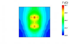
I've been playing with the R-Theta simulation tools trying to determine what the best orientation is for Peter Daniel's F4 boards using the R-Theta 9012 profile in 12" lengths.
I simulated three orientations. The first is with the MOSFET labels vertical, and the second is with the MOSFET labels horizontal and with the N channel devices on top, and the third orientation was horizontal with the P channel devices on top.
The reason for the last two simulations is that the FQA12P20 and FQA19N20C devices have slightly different junction-to-case thermal resistances. For obvious reasons, the first arrangement didn't need to undergo this flip-flopping of devices.
So, what I found via the probably very imprecise tool is the following:
Columns are:
device number (N = FQA19N20C, P=FQA12P20)
power (set to 14.8W per device)
Tsink-average
Tsink-max
Tcase
Tjunction
Simulation #1 (vertical orientation)
N1,14.8 W,48.7,48.9,48.9,75.2
N2,14.8 W,49.5,49.6,49.6,75.8
N3,14.8 W,49.0,49.2,49.2,75.5
P1,14.8 W,48.7,48.9,48.9,77.2
P2,14.8 W,49.5,49.6,49.6,77.9
P3,14.8 W,49.0,49.2,49.2,77.6
Simulation #2 (horizontal orientation, N-channel "on top")
P1,14.8 W,49.1,49.4,49.4,77.7
P2,14.8 W,50.2,50.3,50.3,78.7
P3,14.8 W,49.1,49.4,49.4,77.7
N1,14.8 W,49.5,49.7,49.7,76.0
N2,14.8 W,49.5,49.7,49.7,76.0
N3,14.8 W,50.6,50.7,50.7,76.9
Simulation #3 (horizontal orientation, P-channel "on top")
N1,14.8 W,49.1,49.4,49.4,77.7
N2,14.8 W,50.2,50.3,50.3,78.7
N3,14.8 W,49.1,49.4,49.4,75.6
P1,14.8 W,49.5,49.7,49.7,76.0
P2,14.8 W,50.6,50.7,50.7,77.0
P3,14.8 W,49.5,49.7,49.7,76.0
pictures to follow...


luvdunhill said:so, it looks like orientation #1 is best.
Wouldn't 2 or 3 be preferable - lower peak temperature and more uniform spread across the fets?
jimbo51 said:
Wouldn't 2 or 3 be preferable - lower peak temperature and more uniform spread across the fets?
I don't know. The junction temperate is quite a bit higher. I did some more tests, this time using the first simulation and moving the FETs out and in. Surprisingly, the middle position was the best. I figured getting them furthest apart would be better. I think it has something to do with the heat sink boundary. I'll attach pictures:
Attachments
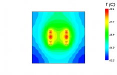
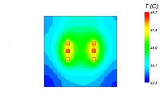
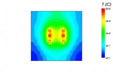
it's easiest if you download all the images in different tabs and switch to compare.. again, probably pseudo-science... I'm sure others have opinions that may be more useful. These last 3 images show about as far as you can stretch the boards with still using the legs of the device. I can post more data if it's helpful...
jimbo51 said:
Wouldn't 2 or 3 be preferable - lower peak temperature and more uniform spread across the fets?
wait, the last 2 have higher temperatures, but more uniform.. right?
anyways, I'm going to relax and watch a movie.. I'll check back in the morning
I thought it was time I finally I gave an update on my F4. I finally got to put my chassis together. I still need to finish up the wiring and add some feet, but I am pretty happy with the results.
http://www.flickr.com/photos/65445808@N00/3014333672/in/photostream/
http://www.flickr.com/photos/65445808@N00/3014333672/in/photostream/
DaveM said:I thought it was time I finally I gave an update on my F4. I finally got to put my chassis together. I still need to finish up the wiring and add some feet, but I am pretty happy with the results.
http://www.flickr.com/photos/65445808@N00/3014333672/in/photostream/
extremely fugly !

luvdunhill said:
wait, the last 2 have higher temperatures, but more uniform.. right?
anyways, I'm going to relax and watch a movie.. I'll check back in the morning
Interesting simulations!

I doubt you'll get really good heat distribution with this placement of fets. Have you tried simulating what happens if you put all the fets on a row like some of the other pcb designs?
luvdunhill said:it's easiest if you download all the images in different tabs and switch to compare.. again, probably pseudo-science... I'm sure others have opinions that may be more useful. These last 3 images show about as far as you can stretch the boards with still using the legs of the device. I can post more data if it's helpful...
Using the same temperature scale on the simulations would also help making comparison easier.
luvdunhill said:so, it looks like orientation #1 is best. Any idea if the last few hours were a complete waste of time or not?
Sure not waste of time, I have spent a fair amount of time on this.
The conclusion you most likely will end up with, is a copper heat spreader, aka a sheet of 10mm copper.
This will offer you close to perfect thermal stability.
The drawback, is that the warm up time is extended by the thermal mass, so it's a matter of preferences.
Magura
cviller said:
Interesting simulations!
I doubt you'll get really good heat distribution with this placement of fets. Have you tried simulating what happens if you put all the fets on a row like some of the other pcb designs?
well, I wanted to try and keep the original Peter Daniel board configuration, and finding the best orientation was sort of the stimulus of this whole things anyways
Magura said:
Sure not waste of time, I have spent a fair amount of time on this.
The conclusion you most likely will end up with, is a copper heat spreader, aka a sheet of 10mm copper.
This will offer you close to perfect thermal stability.
The drawback, is that the warm up time is extended by the thermal mass, so it's a matter of preferences.
Magura
I've thought about this. I was considering strips of copper about the same size as the FETs and 12" long running up the heat sink. What shape would you propose for the spreader? The problem here is as I believe GRollins noted is that a single 12"x12" heat sink is difficult to really use well.
luvdunhill said:
I've thought about this. I was considering strips of copper about the same size as the FETs and 12" long running up the heat sink. What shape would you propose for the spreader? The problem here is as I believe GRollins noted is that a single 12"x12" heat sink is difficult to really use well.
Depending how tight your economy is, the simple solution to make the best of your heatsink, is to get a 10mm thick sheet, and cut it to be able to fit all 6 fets on it, or to cut a 12" by 12" 10mm sheet, which will allow you to mount your fets, just about anywhere you please.
Magura
Heatsink and junction temperatures
Thank you for doing all this work. My take on what you have shown is somewhat different -- they are all essentially the same with only minor differences. Junction temp varying by 3 degrees, center FETs, whether P or N channel, running somewhat warmer than their neighbors. Seriously, I wouldn't worry about it.
It would be interesting however to compare the temperatures for the devices and across the heatsink if the devices were attached in a single row across the length of the heatsink, more or less equidistant from each other and the edges of the heatsink. . .
Thanks for your efforts. It is very interesting.
Steve Z
luvdunhill said:
I don't know. The junction temperate is quite a bit higher. I did some more tests, this time using the first simulation and moving the FETs out and in. Surprisingly, the middle position was the best. I figured getting them furthest apart would be better. I think it has something to do with the heat sink boundary. I'll attach pictures:
Thank you for doing all this work. My take on what you have shown is somewhat different -- they are all essentially the same with only minor differences. Junction temp varying by 3 degrees, center FETs, whether P or N channel, running somewhat warmer than their neighbors. Seriously, I wouldn't worry about it.
It would be interesting however to compare the temperatures for the devices and across the heatsink if the devices were attached in a single row across the length of the heatsink, more or less equidistant from each other and the edges of the heatsink. . .
Thanks for your efforts. It is very interesting.
Steve Z
- Home
- Amplifiers
- Pass Labs
- F4 power amplifier