Off board IV Convertor
Hello,
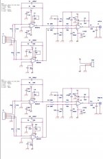
I am building a ezDAC and thought of building a IV convertor with summing stage myself. Here is the schematic which I came up with. It is customizable to support Dual Mono and can work with different filter types.
I am planning on making a PCB for this schematic and open to suggestions / comments.
Hello,
I am building a ezDAC and thought of building a IV convertor with summing stage myself. Here is the schematic which I came up with. It is customizable to support Dual Mono and can work with different filter types.
I am planning on making a PCB for this schematic and open to suggestions / comments.
Attachments
Off board IV Convertor
In my search for "Clean Power Circuits" to feed the Digital and Analog sections, I recently reviewed a document: "Power Supply Noise Reduction" which you can download (PDF) from "The Designers Guide Community" web site. In addition to discussion on Supply bypassing and decoupling... from which I learn that it was best to keep tracks really short, and with the onus on keeping return paths close to the send path, it also covers OP Amp coupling/decoupling choices as being critical.
My plan is to leave the buffer (I/V receiver) OP Amp in it's compact real estate on the EZDac board, simply because I do not feel the risk of increasing RF noise is worth moving that component to the Headphone Amp board (read my lack of confidence here).
I looked up the LT1028 Data and find it to be an excellent choice... in meeting one main criteria which IMO parallels the importance of a well designed circuit board (RF interference free), and that being the settling time. Your schematic print is small, so could not see the part number on the other OP Amp (NE5634A ? could not internet-find a data sheet on that one).
Louis
Hello,
I am building a ezDAC and thought of building a IV convertor with summing stage myself. Here is the schematic which I came up with. It is customizable to support Dual Mono and can work with different filter types.
I am planning on making a PCB for this schematic and open to suggestions / comments.
In my search for "Clean Power Circuits" to feed the Digital and Analog sections, I recently reviewed a document: "Power Supply Noise Reduction" which you can download (PDF) from "The Designers Guide Community" web site. In addition to discussion on Supply bypassing and decoupling... from which I learn that it was best to keep tracks really short, and with the onus on keeping return paths close to the send path, it also covers OP Amp coupling/decoupling choices as being critical.
My plan is to leave the buffer (I/V receiver) OP Amp in it's compact real estate on the EZDac board, simply because I do not feel the risk of increasing RF noise is worth moving that component to the Headphone Amp board (read my lack of confidence here).
I looked up the LT1028 Data and find it to be an excellent choice... in meeting one main criteria which IMO parallels the importance of a well designed circuit board (RF interference free), and that being the settling time. Your schematic print is small, so could not see the part number on the other OP Amp (NE5634A ? could not internet-find a data sheet on that one).
Louis
Hi Louis
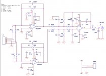
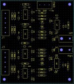
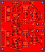
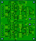
The other op-amp is the good old NE5534A. In fact I just completed the routing the board and its about the size of 3x3.5in. I am still debating on whether to include a clean power supply section along with the board.
I have attached one half of the schematics in a readable size.
The other op-amp is the good old NE5534A. In fact I just completed the routing the board and its about the size of 3x3.5in. I am still debating on whether to include a clean power supply section along with the board.
I have attached one half of the schematics in a readable size.
Attachments
[ Well I guess it would be the next logical step. What do you think on these ?
DualReg
Relieved to see I am not alone in a search for an "easy to do" or inexpensive
low noise regulator circuit. I must admit not having come across the one you show here. Would like to see the circuit. One comment on one component I see on the board... really have a strong dislike for the "cheap" adjustable resistors: brings back memories on their causing loss of transistors when making bias adjustments... the film therein goes bad in this planet's oxygen atmosphere; maybe what I see is not one of those?
Louis
The trimmer is a bit cheap indeed, I'd rather use one with fixed resistors. But the Reg itself could be a quick-and-easy upgrade for the standard 78xx/79xx ones. Price is not steep, noise is low compared to standard regs, although it would be nice to know what they do beyond 20kHz. The 40mA maximum current could be a problem with the digital section of the ezDAC though, IIRC it needs more than that.
Ray
Ray
Hello,
I am building a ezDAC and thought of building a IV convertor with summing stage myself. Here is the schematic which I came up with. It is customizable to support Dual Mono and can work with different filter types.
I am planning on making a PCB for this schematic and open to suggestions / comments.
Looks very good, this topology can be used for lots of current-out DAC's. Personally, I wouldn't pick the NE5534 though
 . But if you fit some sockets, you can do some opamp-rolling, it's a lot of fun and can be very revealing!
Ray
Hi Louis
The other op-amp is the good old NE5534A. In fact I just completed the routing the board and its about the size of 3x3.5in. I am still debating on whether to include a clean power supply section along with the board.
I have attached one half of the schematics in a readable size.
Looking at the ezDAC board, the I/V resistors are advantageously close to U3.
Would it be OK to use those positions rather than place them some distance on the HPhone Board? I may be off track when considering the benefit of a voltage signal vs a current feed over some distance? The current running to the adjacent board creates a magnetic field around the "longer" conductor; such field would be of a lesser intensity with the smaller current drawn by the receiver OP Amp if sensing a voltage feed on those same conductor wires? Is the very nature of capacitance and inductive coupling problems not current dependent? On the other hand, RF/AC fields (any frequency) are lazy by nature and will prefer hitching a ride through a shunt like a copper track/wire, thus inducing noise current... so which approach would be less risky for noise pick-up?
Louis
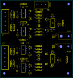
Ray for the very same I decided to use DIP package on the board which gives you an option to playaround with OpAmp of you choice. I will post the board design images.
Looks very good, this topology can be used for lots of current-out DAC's. Personally, I wouldn't pick the NE5534 though
Ray
I understand your concern about the capacitance and inductive problems. I have done some experiment in the past and as long as you keep the wires as short as possible and avoid crossing power supply wires, then you should be good.
Another interesting thing with this design is, its easy to get a differential out if you use two of them.
Another interesting thing with this design is, its easy to get a differential out if you use two of them.
Looking at the ezDAC board, the I/V resistors are advantageously close to U3.
Would it be OK to use those positions rather than place them some distance on the HPhone Board? I may be off track when considering the benefit of a voltage signal vs a current feed over some distance? The current running to the adjacent board creates a magnetic field around the "longer" conductor; such field would be of a lesser intensity with the smaller current drawn by the receiver OP Amp if sensing a voltage feed on those same conductor wires? Is the very nature of capacitance and inductive coupling problems not current dependent? On the other hand, RF/AC fields (any frequency) are lazy by nature and will prefer hitching a ride through a shunt like a copper track/wire, thus inducing noise current... so which approach would be less risky for noise pick-up?
Louis
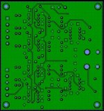
Hi,
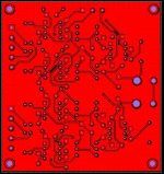
Looks good, but it looks like your TOP layer groundplane (red) is not connected to anything. There's a long trace running on that layer connecting all the ground points, but that's actually not needed as everything is already connected through the BOTTOM layer copper plane and plated holes. Are you using a netlist from the schematic? Otherwise this wouldn't be possible.
Ray
Want an "adequate dual regulator" choice?
Agree the "trimmer" seen on the referenced board can be upgraded, so would consequently like to learn more on this regulator circuit. I have reviewed several circuit topologies, and am looking for a design that is simple and adequately suitable in performance without reaching way down in the dB dungeon (how low is low enough?). Perhaps an excellent compromise would be the " No-Feedback Voltage Regulators" topology set forth by Andy Nehan in AudioXpress 10/01... wherein the author makes use of a FET pass element.
At the end of the day, will want to "roll a proven design" w/o going the route of the super topology.
Would appreciate other thoughts/experience on this...
Thank you,
Louis
No Feedback Regulators
Hello Ray,
Could not locate a PDF version of the AudioXpress article, but can summarize the author's approach here:
1. Avoids the usual regulators such as LM317, etc. because of their inadequacy in maintaining a steady output impedance versus frequency, & as generators of noise.
2. Avoids returning noise back into the input side of a regulating circuit.
3. Uses RC filters to remove a good portion of Rectifier/Power line noise... down to an acceptable level (with 2 poles being sufficient).
4. Uses what appears to me like "capacitance multiplier" circuit based on a FET pass element (i.e. IRF840). This applies for positive rail regulation.
5. Uses BJT as pass element for the negative rail regulation.
6. Both regulating circuits use current sources and zeners.
I could not see any resemblance with the Teddy Regulator(s).
Louis
Hi Louis,
Well, good thing I noticed the resemblance then
1. The Super Teddy Reg is not an LM317, uses no feedback and has very low noise
2. ???
3. An input filter is not part of the STR, but nonetheless this can be accomplished
4. It uses two cap. multipliers
5. It uses an NPN transistor, which is a BJT
6. It uses a discrete zener with LED as reference
Regards,
Ray
- Status
- This old topic is closed. If you want to reopen this topic, contact a moderator using the "Report Post" button.
- Home
- Source & Line
- Digital Line Level
- ezDAC v.1.5 Builders Thread