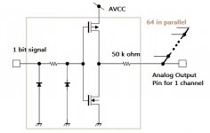
Possible equivalent circuit schematic for ES9018 analog output
(This post is not related to Shinja's previous post.)
In a local BBS in Japan, Shinja and Bunpei recently have discussions on a possible equivalent circuit schematic for ES9018 analog output section.
Bunpei summarized the result and posted here. Does anyone have his/her own alternative interpretations for the analog output section of ES9018 architecture? We welcome your frank comments. It's just a "sand bag" version.
Main points for our guess are;
1. Delta-sigma modulated 64 level sound intensity information is decomposed to 64 of 1 bit digital switching signals. ( DEM should be incorporated for a selection of switches.)
2. A usual and simple C-MOS logic circuit constitutes one 1 bit digital switching circuit shown in the attached picture. The output signal goes through one 50 k ohm resister in serial. There might be no elaborated AVCC regulation circuit.
3. Outputs of totally sixty four 1 bit digital switching circuits are connected in parallel to a single analog output pin of one polarity of one channel. No analog filter circuit is placed before the output pin. No switched capacitors are included.
Attachments
Last edited:

Bunpei, interesting idea!
I am also interested in knowing the exact way the output stage look like in the ESS9018.
Let´s see if I understand what you have drawn. To the left comes the signal, ie the music in digital form, and then the signal is made analog and the output is at the far right with a 50k resistor in series with the output; the 50k / 64 = 781.25 Ohms, which is the output resistance of the ESS9018 in stereo mode setup. Correct?
Could you maybe draw the waveforms on the input and output including any DC offset level?
My question is if there is any positive affect in having the output stage draw DC current. This can be prevented by a cap in series with the output, use a transformer, or by setting the I/V converter´s voltage to VACC/2 instead of GND.
/S
(This post is not related to Shinja's previous post.)
In a local BBS in Japan, Shinja and Bunpei recently have discussions on a possible equivalent circuit schematic for ES9018 analog output section.
Bunpei summarized the result and posted here. Does anyone have his/her own alternative interpretations for the analog output section of ES9018 architecture? We welcome your frank comments. It's just a "sand bag" version.
Main points for our guess are;
1. Delta-sigma modulated 64 level sound intensity information is decomposed to 64 of 1 bit digital switching signals. ( DEM should be incorporated for a selection of switches.)
2. A usual and simple C-MOS logic circuit constitutes one 1 bit digital switching circuit shown in the attached picture. The output signal goes through one 50 k ohm resister in serial. There might be no elaborated AVCC regulation circuit.
3. Outputs of totally sixty four 1 bit digital switching circuits are connected in parallel to a single analog output pin of one polarity of one channel. No analog filter circuit is placed before the output pin. No switched capacitors are included.
... To the left comes the signal, ie the music in digital form, and then the signal is made analog and the output is at the far right with a 50k resistor in series with the output; the 50k / 64 = 781.25 Ohms, which is the output resistance of the ESS9018 in stereo mode setup. Correct? ...
Yes, I think your understanding is correct.
... Could you maybe draw the waveforms on the input and output including any DC offset level? ...
I'm not sure whether the schematic can explain the DC offset, AVCC/2 or not.
Any improvements on the schematic by audiences are appreciated.
@ staccatiss: no, the output resistance/impedance is 195Ω in stereo mode, its 781Ω in 8 channel mode, so 781Ω || 781Ω || 781Ω || 781Ω = 195Ω, which I think is what you meant to say anyway yes? the above represents only one phase of one of the 8 dac channels. there are 1024 x 1 bit dacs in the ES9018 afaik.
being an only VEE+ dac, are you sure its CMOS? I thought perhaps it was an all N-channel arrangement, but thats not something i've given much thought, since we can only guess I hadnt bothered, Dustin is hardly going to pop in and tell us. that would explain the offset more readily though.
edit: actually, how could it not have an offset with only VEE+ supplies? it has to swing around the middle of 0->+3.3V for a balanced output, so how could the middle be zero?
Last edited:
In this assumption,
I also assumed the distortion source at voltage output mode ,which may be on resistance variation of MOSFET and thermal modulation of 50kohm resistance.
Thermal modulation distortion may become a problem at current output mode when output pin is fixed 0V with virtual short, instead of 1/2AVCC.
The distortion will be mainly 2nd order ,thus they are almost canceled out by summing differential signal.
However I prefer setting noninverting input 1/2AVCC .
Yes, Zout should be 195.3125 Ohms.
Sure, the output vill swing around around a DC offset (current or voltage depending on load).
Attached is how I have extended Bunpei´s schematic. What I am interested in knowing, is what curents pass through the MOSFETs with different R3 and different V_IV.
The question is then how does the MOSFET buffer (inverter) look like?
@ staccatiss: no, the output resistance/impedance is 195Ω in stereo mode, its 781Ω in 8 channel mode, so 781Ω || 781Ω || 781Ω || 781Ω = 195Ω, which I think is what you meant to say anyway yes? the above represents only one phase of one of the 8 dac channels. there are 1024 x 1 bit dacs in the ES9018 afaik.
being an only VEE+ dac, are you sure its CMOS? I thought perhaps it was an all N-channel arrangement, but thats not something i've given much thought, since we can only guess I hadnt bothered, Dustin is hardly going to pop in and tell us. that would explain the offset more readily though.
edit: actually, how could it not have an offset with only VEE+ supplies? it has to swing around the middle of 0->+3.3V for a balanced output, so how could the middle be zero?
Attachments
ES9018 in Merging Horus
Some people active on this forum may know that Horus AD/DA unit of Merging Technologies began to support DSD256 recording/play capabilities with Pyramix 8.1 software last April.
On Computer Audiophile Forum, tailspn, his real name is "Tom Caulfield" and one of Grammy Awards 2013 winners, a user of Horus/Pyramix system, revealed that the unit incorprates;
- ESS Technology, ES9018 for DA
- Arda Technologies, AT1201 for AD
in the thread,
To DSD or not to DSD? - Page 19
staccatiss,
your figure have an error.
if you treat the resister as 195ohm, the signal source must be treated as 64level.(or 128,256,512 level according to quantizer resister)
Each 1bit DACs output AVCC or GND level.
Our assumption is previously described in this post.
http://www.diyaudio.com/forums/digi...-reference-dac-8-channel-134.html#post1761129
your figure have an error.
if you treat the resister as 195ohm, the signal source must be treated as 64level.(or 128,256,512 level according to quantizer resister)
It is just a switch.how does the MOSFET buffer (inverter) look like?
Each 1bit DACs output AVCC or GND level.
Our assumption is previously described in this post.
http://www.diyaudio.com/forums/digi...-reference-dac-8-channel-134.html#post1761129
Last edited:
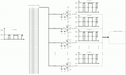
New schematic attached. Now there are 64 one bit DAC:s. I do not know much about the internals of a DAC, so I think there is still somethign missing in my schematic. This schematic cannto give out music, or?
Yes, I think your understanding is correct.
I'm not sure whether the schematic can explain the DC offset, AVCC/2 or not.
Any improvements on the schematic by audiences are appreciated.
Attachments
Last edited:
Play with "No bandwidth" on DPLL setting
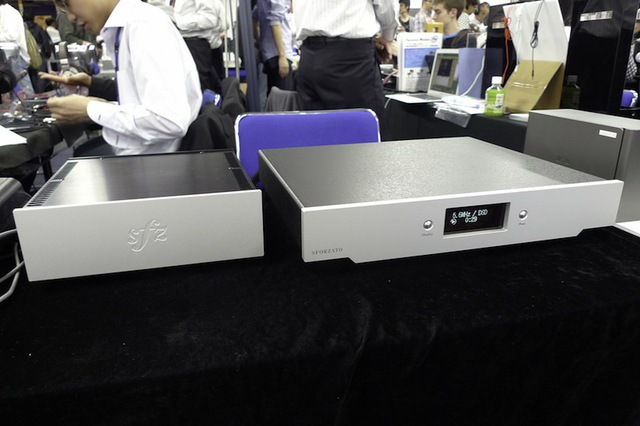
A Japanese manufacturer, "SFORZATO Corporation" will release a network player product, DSP-03, this month.
SFORZATO_DST_Detail (in Japanese)
They use ES9018 chips and they say that a play with a DPLL parameter "No bandwidth" is achieved in the player. Bunpei asked the developer what a mechanism has made it possible. His brief answer was;
"A reclocking of I2S/DSD signals with a synchronous MCLK just before the inputs to the DAC chips."
I dont believe them, it doesnt work with fifo, which is synchronous and VERY low jitter, but my understanding is that the DPLL setting is meaningless with sync mode clocking anyway, as the DPLL should be doing nothing, so whats the point? Dustin himself has mentioned that in sync mode the DPLL is 'freewheeling' so sorry I think this is marketing spin. even if it is true, it doesnt mean anything, truly synchronous operation would not need the DPLL of any bandwidth.
If they REALLY have archived no_dpll_bandwidth stable without dropouts,
distributing/reclocking differential signal (ECL?) might be a key to no_bandwidth_stability, - that should be what no one have tried before -
Just an assumption.
I will try with NDK ECL in a few weeks again just to be sure, but I think this is purely academic
ES9018-2M Sabre32 Reference Stereo DAC
Has anyone obtained a datasheet of this new model?
http://www.esstech.com/Pr_2013/ES9018-2M%20%20PR%20130621.pdf
Has anyone obtained a datasheet of this new model?
http://www.esstech.com/Pr_2013/ES9018-2M%20%20PR%20130621.pdf
Hi guys,
I am an ES9018 fans and a DSD lover. I saw a video from ESS Sale Office(China) recently, Mr. Zhang said that the 9018 isn't 1bit DSD DAC chip, and DSD to PCM conversion will be done in 9108(i disbelieve it, maybe a big confusion?).
I got other opposite informations from computeraudiophile.com about this. Mr. Michal who is the designer of Mytek, here are his words:
"Ok,the way DSD is implemented in our DAC:
DSD 1 bit> digital DSD 3 pole filter @ selectable 50,60 or 70kHz>6 bit output > 6 bit DAC. The filter, standard in all sacd players (typically analog) helps to filter out of band noise inherent n DSD. Such filtering requires multiplication which produces result in more bits than the 1bit input. It's actually in away better than 1 bit because all info is preserved but 6 bit conversion is more accurate than 1 bit. It's better to keep it at 6 bits than round it to 1 bit, for example. We are still talking about 64xFS stream of 6 bit data , NOT any PCM."
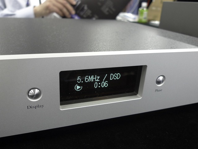
According to Mr. Michal's descriptions, the ES9018 does 6-bit SDM and the DSD SR is still 2.8M(or 5.6M), No any PCM.
Who is right?
Thanks!
I am an ES9018 fans and a DSD lover. I saw a video from ESS Sale Office(China) recently, Mr. Zhang said that the 9018 isn't 1bit DSD DAC chip, and DSD to PCM conversion will be done in 9108(i disbelieve it, maybe a big confusion?).
I got other opposite informations from computeraudiophile.com about this. Mr. Michal who is the designer of Mytek, here are his words:
"Ok,the way DSD is implemented in our DAC:
DSD 1 bit> digital DSD 3 pole filter @ selectable 50,60 or 70kHz>6 bit output > 6 bit DAC. The filter, standard in all sacd players (typically analog) helps to filter out of band noise inherent n DSD. Such filtering requires multiplication which produces result in more bits than the 1bit input. It's actually in away better than 1 bit because all info is preserved but 6 bit conversion is more accurate than 1 bit. It's better to keep it at 6 bits than round it to 1 bit, for example. We are still talking about 64xFS stream of 6 bit data , NOT any PCM."
According to Mr. Michal's descriptions, the ES9018 does 6-bit SDM and the DSD SR is still 2.8M(or 5.6M), No any PCM.
Who is right?
Thanks!
- Home
- Source & Line
- Digital Line Level
- ESS Sabre Reference DAC (8-channel)