Hi Bunpei
I noticed about your hope to have me her as read-only member, and I hope too that I will not disappoint you very much in your hope, answering (writing actually) yours above post, and precise for you and others that may CLAIMS reefers to my experiments, and reflect my experienced events (results) in this connection. I do not claim that doing so, or follow my ways, one or everybody will be happy forever with the same results. Also I do not have any possibility to control how and what somebody else who read my "claims" do it with theirs gears, equipments or devices.
I found out about something, I experienced so an so, I had/have so and so results and I came here to inform the others who may eventual be interested, about that. The same you did and many another too.
It is enough unfortunate that some can not distinguish between "claims" and informations.
what are the limits on AVCC voltage and large capacitor decoupling?
One of the few references to AVCC are:
http://www.esstech.com/PDF/sabrewp.pdf said:17 With 4.0V power supply greater than 133dB can be achieved.
http://www.esstech.com/PDF/sabrewp.pdf said:Therefore, the node labeled AVcc (the analog power supply) might better be called “DACReference” since it is the DAC reference level. You will note in our recommended PCB designs that either an amplifier or a large capacitor is placed at the Avcc point to ensure that the noise is not reduced by any spurious signal at this point.
For those that have the data sheet there are more details there.
I have been running AVCC at 5.5 volt and clocks at 90.3168/98.304MHz for at least 2.5 years - and the operation and performance are still superb.
However I know of others that have destroyed the DAC chips at lower voltages than my used 5.5 volt, and I have "heard" of performance issues above 4 volt.
As I use the LU1014D JFET as the regulator output device and when powering up the voltage do never "spike" above the 5.5 volt, and voltage spikes on the mains etc. can never "spike" the AVCC above the 5.5 volts.
If a voltage regulator (with feedback (they all have feedback)), a OPAmp or a shunt regulator are used - and there will always be "spikes" above the "normal" output voltage.
The limits of the size of a decoupling capacitor depends on the regulator topology used. The above mentioned voltage regulators, OPAmps or shunt regulators are shorted by the decoupling capacitor at power on and may not function correctly with huge decoupling capacitors.
I have used 1F (1.000.000uF/5.5 volt) with my LU1014D regulators without issues. For voltages below 2.5 volt I even have used 10F (10.000.000uF/2.5 volt). OS-CON banks up to 4.700uF and standard electrolytic up to 120.000uF have been used without issues. It is the regulator topology that matters and not the used DAC chip model. I started using the 1F capacitors with Burr Brown DAC chips more than ten years ago, and with the passive regulators I used at that time it took 15 minutes for the 5 volt rails to reach (charge) a stable voltage, and I had to reset the DAC chips to calibrate the internal reference circuits.
There are one issue that may cause problems with huge capacitor values...
When powering off - the capacitors (if huge values) may not discharge properly in all instances and when powered on again this may cause havoc..
The internal "reverse" diode in the LU1014D effectively discharges the capacitors when the input voltage to the LU1014D goes low.
I do NOT recommend modifying existing designs by changing the used voltages or adding huge capacitor values..
If you want to experiment with "out of spec" values you should make your own design. If you are not capable to make a DAC design from scratch then you should leave that to others..
In regard of oscillator frequencies above "spec" I have tested several different DAC chips. As the oscillator frequency rises the noise generated by the DAC chip rises and the performance of the DAC chips declines..
With a Sabre DAC you must measure and listen to the DAC directly without any I/V or passive filter attached. I discovered then easily that over clocking reduced both fidelity and the measured performance.
It were happened that you destroyed an ESS9018 ever, because to high AVCC? If so, or if you know about, can you say what it may be the highest level for AVCC on this DAC chip?
I did not known that ESS9018 can tolerate so high AVCC. Datasheet mention about 4v. I just wonder what is the absolute (in fact) limit of AVCC.
When about over clocking I run, it result out of this my setup an audio signal (final opamp out) of approx. max 26Vpp, and an residual noise (in to few teens Mhz and constant level - independent of the useful signal) of 0,6Vpp. I found an way (no filtering) to reduce that residual noise to 32mVpp on RCA output, for an audio signal of max 18-20Vpp at the same point. I could not notice any reducing in fidelity, but opposite.
Without I/V stage you meant to connect the DAC output directly to an amplifier, or an buffer in between?
I did not think to try this way, but I will do it to compare the results.
Else I will point out that using an voltage regulator with large capacities on output, it will prevent anyway the eventual spikes on power ON sequence. An good quality/designed regulator will not have such spikes. The only thing one may care in this case is that the regulator be over current protected... The most are.
(Sorry for not been (yet) an read only member...)
Last edited:
It were happened that you destroyed an ESS9018 ever, because to high AVCC? If so, or if you know about, can you say what it may be the highest level for AVCC on this DAC chip?
I did not known that ESS9018 can tolerate so high AVCC. Datasheet mention about 4v. I just wonder what is the absolute (in fact) limit of AVCC.
I do not know the limits...
I had one application where I needed 5 to 5.5 volt AVCC - using a Tripath modulator as I/V.
The Sabre have 800 / 200 ohm output and can drive the Tripath modulator DC coupled if the AVCC are high enough to be able to match the DC output to the DC input of the Tripath chip. It worked and no chips have been destroyed in this experiment.
When about over clocking I run, it result out of this my setup an audio signal (final opamp out) of approx. max 26Vpp, and an residual noise (in to few teens Mhz and constant level - independent of the useful signal) of 0,6Vpp. I found an way (no filtering) to reduce that residual noise to 32mVpp on RCA output, for an audio signal of max 18-20Vpp at the same point. I could not notice any reducing in fidelity, but opposite.
Without I/V stage you meant to connect the DAC output directly to an amplifier, or an buffer in between?
I did not think to try this way, but I will do it to compare the results.
The I/V stage and analog filters "removes" most of the noise above xxkHz (depending on the I/V and filters), but some of this noise will add to the signal and will change the audio "signature". More energy / level are most often falsely identified as "better"...
By testing the over clocking without a I/V stage and without any filters you will be able to measure and also "hear" the real added noise...
Else I will point out that using an voltage regulator with large capacities on output, it will prevent anyway the eventual spikes on power ON sequence. An good quality/designed regulator will not have such spikes. The only thing one may care in this case is that the regulator be over current protected... The most are.
Then you must look into some data sheets and see what happens when a regulator with feedback are "loaded"...
The feedback tries to increase the output voltage and what happens is just the same as clipping in a feedback amplifier.
The feedback are shorted and the regulator "gain" are open loop and will drive the voltage up and create spikes...
I have even seen the regulator start oscillating and thus creating a "signal" overlaid the DC output level...
RayCtech,
Thanks for all the details. 1F!, Those are for car stereo enthusiasts
Reminds me of the MDAC with a bunch of high value caps surrounding the ES9018 chip...
 Properly done (the whole design) it actually sounds more valve than a valve amplifier (and have the bass and highs included) and have more control (and better fidelity) than McIntosh 2kw mono blocks.
The only amplifiers I have tested that are slightly better in fidelity are the class A JFET amplifiers

Inverted MCLK
Guys, would you please speculate about the ESS recommendation for inverted MCLK in sync mode?
IMHO, inverted MCLK is needed for taking into consideration the propagation delays at the I2S source if the clock is tightened to the DAC and remotely controls the source.
What are your opinions?
Guys, would you please speculate about the ESS recommendation for inverted MCLK in sync mode?
IMHO, inverted MCLK is needed for taking into consideration the propagation delays at the I2S source if the clock is tightened to the DAC and remotely controls the source.
What are your opinions?
Last edited:
The only amplifiers I have tested that are slightly better in fidelity are the class A JFET amplifiers
Hi,
My experience with power supplies has shown me that I want a regulator with extremely low output impedance, and minimal capacitance, rather than trying to create such low z with a bank of capacitors. It sounds like it reacts faster and has no colouration, such as valve-like sound.
In the case of a capacitor bank, the choice of capacitor becomes the dominant force in the colouration of the sound, so then I want to use film caps, not electrolytics or polymer. And then really good film caps.... And then it gets horribly expensive. Plus Mundorf silver/oil are just huge. ;-)
So I thought I'd add my opinion and see if you agree that a low z supply is better than a colourful ton of caps ?
Last edited:
... I have used 1F (1.000.000uF/5.5 volt) with my LU1014D regulators without issues. For voltages below 2.5 volt I even have used 10F (10.000.000uF/2.5 volt). OS-CON banks up to 4.700uF and standard electrolytic up to 120.000uF have been used without issues. ...
You must have added five more 470 uF OS-CONs to the prototype version you have shown us before and located the board near to your DAC chip.
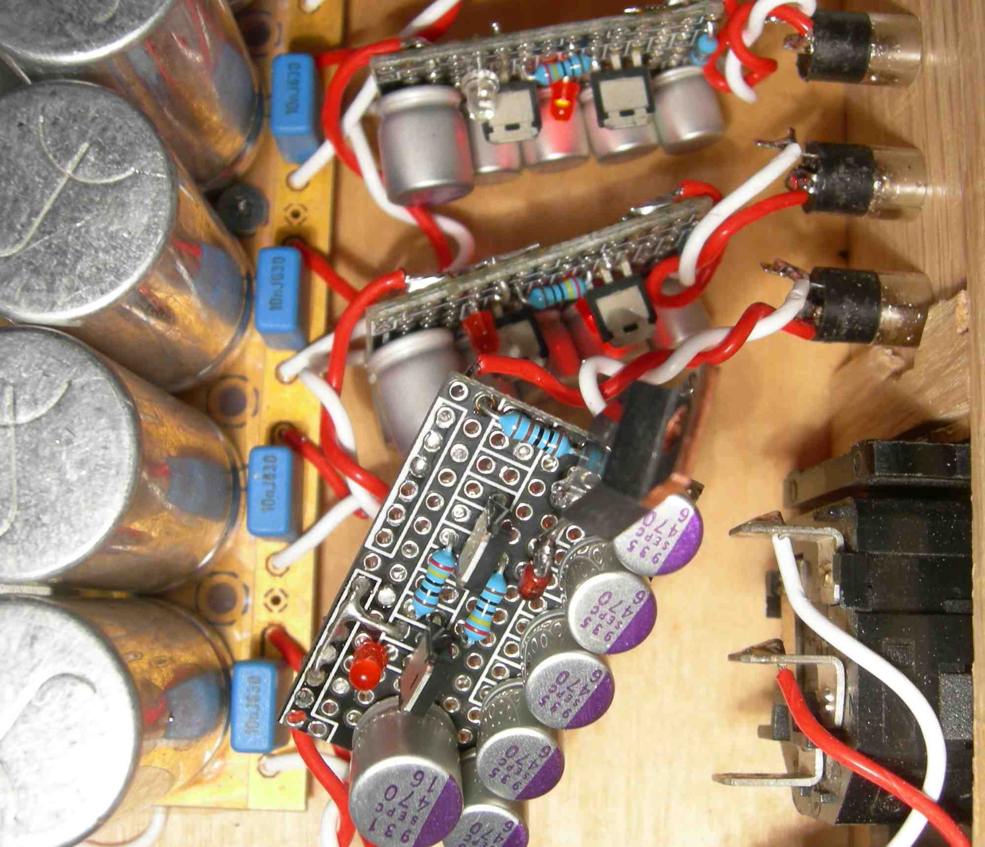
You must have added five more 470 uF OS-CONs to the prototype version you have shown us before and located the board near to your DAC chip.
Hi Bunpei,
That was a small part of an really old and now obsolete setup
Actually it was only the main PSUs (pre-regulators) for an USB adapter, I2S isolator and the LVDS (I2S) transmitter boards
The current (soon yet another revision to be finished) DAC board alone there are 30 pcs of the 470uF OS-CONs..
Even this version are over a year old design and I think it stretched the ES9018 to the absolute technological limits as it implemented the 9bit true mode...
As soon as that project are ended I will finish my newest creation:
A DAC that supports DSD up to and including DSD2048 and PCM up to and including 3072k/32bit. Runs in NOS mode or modes with up sampling up to 256x.
Last edited:
As soon as that project are ended I will finish my newest creation:
A DAC that supports DSD up to and including DSD2048 and PCM up to and including 3072k/32bit. Runs in NOS mode or modes with up sampling up to 256x.
What DAC chip supports that?
As soon as that project are ended I will finish my newest creation:
A DAC that supports DSD up to and including DSD2048 and PCM up to and including 3072k/32bit. Runs in NOS mode or modes with up sampling up to 256x.
Could be nice to see some of your creations... If not as schematics, maybe as pictures at last.
I know RayTech is a very capable engineer, but that sounds like he is kidding
He is not...

RayCtech it seems to be the first one ever who come with such figures as in the post above.
It will be really very interesting for all of us, and for sure the best contribution ever in this forum, if he will accept to come out with some details to make us understand, how is possible (what technology is based) to realize such performances.
Else, I just ordered 2 caps 0,4F/0,04ohm to start my experiments using those on ESS9018. Quite excited about this idea...
... it seems to be the first one ever who come with such figures as in the post above. ...
He wrote his "dRaydream" for the first time here on Amanero thread.
http://www.diyaudio.com/forums/vendors-bazaar/216474-usb-i2s-384khz-dsd-converter-28.html#post3160827
After three months he seems not to be at the phase of publishing his achievements on his own web site.
He wrote his "dRaydream" for the first time here on Amanero thread.
http://www.diyaudio.com/forums/vendors-bazaar/216474-usb-i2s-384khz-dsd-converter-28.html#post3160827
After three months he seems not to be at the phase of publishing his achievements on his own web site.
If I should publish every small detail I had to hire a publisher And the web site was actually terminated sometime last year due to it had not been updated in close to 5 years, and even the AMTs had not been mentioned there
As we "speak" am I listening to native DSD in standard mode (DSD supported up to DSD2048 speed)
I am today debugging a completely new implementation of the USB 2.0 / 3.0 isolation with the OEM Amanero USB adapter and are also debugging the mute output function (timing) of this adapter...
I must add that the improvements in fidelity are remarkable when playing DSD with USB isolation
Last edited:
I know RayCtech is a very capable engineer, but that sounds like he is kidding
12288kHz/32bit was the capability in the initial (PECL) hardware design (and may even possibly still work), but a bit clock at 786.432MHz was a bit overkill. 3072kHz/32bit are realized by splitting data to two data streams - R and L at 32FS clocking - and a bit clock at 98.304MHz. Also 6144kHz/16bit and 12288kHz/8bit can be supported in dual mono 16FS and 8FS mode as the bit clock would still be 90.3168/98.304MHz.
However word clock support up to 12288kHz was kept and a enhanced DSD mode using the whole 32bit data path width can be clocked in by feeding the DSD bit clock to the word clock input. Then DSD64 and DSD128 can be oversampled to DSD256 etc. etc..
Else, I just ordered 2 caps 0,4F/0,04ohm to start my experiments using those on ESS9018. Quite excited about this idea...
Please post a video on Youtube of your psu as you switch on. ;-)
- Home
- Source & Line
- Digital Line Level
- ESS Sabre Reference DAC (8-channel)