tubesguy, Thank you for the link. Just finished reading the thread.
It is useful information, but about what I would expect. The output stage inside a Q2M has to be a down-scaled version of what is in the PRO chip in order for it to be practical for use in cell phones and other mobile devices.
However, the Q2M internal front end is much more similar or perhaps the same as two channels out out of the eight channels of a 9038PRO chip. The ASRC is better in the newer chips and they support more high sample rate modes. A lot has changed in the front end since 9018.
On the other hand 9028PRO and 9038PRO are pretty close, differing for most purposes in output stage current.
It is interesting that everyone still seems to be struggling to find the best solution for AVCC. LifePO4 batteries seem to be a favorite.
In that regard I'm sure there are some who will say there is no measurable difference in DAC performance between some of the AVCC options so it is impossible for there to be any audible difference. I am continuing to come more the view that those people are talking about nonlinear distortion, and the AVCC differences must amount for measurement purposes to linear distortion. In other words, small differences in AVCC power sources do not create measurable amounts of new frequencies. Presumably, they must create some type of linear distortion that we aren't as good at measuring, or that we have not been trying to measure.
Figuring out how to measure the differences is something we should probably get better at. That, and correlating measurements with human perceptual ability. We should also try to better understand perceptual objectionable-ness of linear distortion mechanisms.
From the way people describe differences in AVCC power sources, it seems rather similar to the way they describe audible dielectric absorption characteristics of capacitors. often referring to ESR. Yet, from what we know about dielectric absorption what happens inside capacitors is functionally equivalent to what an RC ladder network does. Low ESR reduces settling time of the equivalent ladder network.
To the extent the ladder network model holds, and there is reason to believe that it holds quite well, that suggests using parallel low-ESR caps connected with minimal resistance interconnections to AVCC pins in combination with the use of a high quality, output-capacitance-tolerant AVCC power supply might a very good thing to try.
Last edited:
I to V converter without GNFB. Sorry, I do not use LT-spice.
No global feedback maybe, but certainly *lots* of local negative feedback. If it sounds good, probably not because of the reasons attributed to it.
Yes, I believe the LT1054 is for the dual rail. The OPA2134s feed into an OPA1622 (tiny black square behind the headphone jack). The clock, yeah, I don't know.. However, right next to it is I think a schmitt trigger inverter ('U20') (?). Curious what that does.
But after lots of comparing, the Hifime sounds much better than the Topping. In fact, the Hifime doesn't sound quite like a typical ESS, reminds me more of an AKM; bolder, more 'musical', mid-centric. Not sure why. THD compensation? Gain compensation? Filter?
Hi, the Hifime dac only uses one opamp without any surrounding filtering caps, I wonder if its working in voltage mode which maybe the reason it sound better than a typical opamp i/v found in the Topping.
In addition, I see Topping uses the tps5130 triple output switcher. I wonder if that supplies the dac chip or just the lcd.
I also see a lot of zero ohm resistors on Topping, could those be replace with chokes to further improve noise?
Even though you prefer Hifime for sound, I am thinking the Topping might make have better modding potentials.
Also, have you tried the various digital filters on the Topping?
47k resistor at the output would be to discharge any output capacitor on the DAC if there were also an input capacitor at the power amp input or other load connected to the DAC output. Otherwise there would be two capacitors in series with an undefined voltage where they connect. Also, it might make a popping noise if a cap were charged and then a cable plugged in to make a connection while the power is on.
Hi, the Hifime dac only uses one opamp without any surrounding filtering caps, I wonder if its working in voltage mode which maybe the reason it sound better than a typical opamp i/v found in the Topping.
In addition, I see Topping uses the tps5130 triple output switcher. I wonder if that supplies the dac chip or just the lcd.
I also see a lot of zero ohm resistors on Topping, could those be replace with chokes to further improve noise?
Even though you prefer Hifime for sound, I am thinking the Topping might make have better modding potentials.
Also, have you tried the various digital filters on the Topping?
The Hifime has 2 OPA2134 opamos feeding an OPA1622. True there are no obvious filtering caps. The board is also populated underneath so perhaps they are there. It's also why it's a little tricky for me to figure out more about the layout. Very compact with tiny SMDs and I do NOT want to fry this dac.
I tried the Topping filters. Interesting, but overall not that impactful. But that's with HD 599 headphones. My 2 channel is inaccessible for testing unfortunately.
Yes for modding the Topping would probably be easier, except for the clocks.
Been doing some more trying and testing here. Currently have the 5v on an external supply and all the power supplies are floating from earth ground, so there is only one earth ground at the moment that comes through one USB connector.
As is happens, there is a wireless phone it the house and it is a DECT system and the base station is about 10ft away from where I am testing the DAC. The DAC sounds better with the phone base station power plug disconnected. I can see some spurs go away in the FFT spectrum too when that happens. Not being in a case, the exposed LME49720's are sensitive to RF. Nothing new there, they are known to be sensitive in that way. It is just that it is more of a problem in terms of audibility than I previously expected.
So far so good. So, decided to try a couple more experiments. At the moment the DAC is sandwiched top and bottom between some thick aluminum plates, with some thinner plates shielding the sides. Sounds better, less distorted. Similar effect to turning off the DECT phone base station. Haven't checked but probably even fewer and lower level FFT spurs.
Also, tried sticking a small heat sink on the differential stage opamp. Cut off one end of a heat sink for 14-pin ICs to make it fit although its still a little longer than the op amp. Stuck it on with some thermally conductive tape. It is okay to the touch now.
Think I will try rigging heat sinks to the IV opamps and see what happens there.
Right now the sound is very clear and detailed. It could not be as detailed if there were any appreciable distortion. I tried playing the first song on the Steely Dan Aja album from CD but upsampled to 24/192, which I happen to be familiar with (production-wise). I can distinctly hear the individual voices of the back up singers, and when the high hat cymbal is struck it sounds distinct and very different from the ride or the crash. Lots of little details are there very similar to what the same song sounds like on the Benchmark DAC-3. Individual sounds are close to as distinct as they are on DAC-3. One doesn't have to expend effort to make them out, they are just there. (Perhaps if someone never heard something like that before they could have no way of knowing just how much information is actually encoded on a CD.)
I am starting to wonder if I just put some heat sinks on the IV op amps, and started hooking the power supplies back up normally, what would happen. In other words, I think it is fine aside from remaining IV op amp heat. It will need a sturdy, probably not-too-thin steel case, maybe similar to DAC-3 and careful attention to making sure it is an effective RF shield.
Then if it passes measurements and listening tests I think I could call it finished and done. If. Otherwise more work to do.
As an aside, FFT spurs were much lower at Richard Marsh's, no more than -130dB. Otherwise I don't think it would have measured as well, it couldn't have. Pretty sure RF in the vicinity causes increased harmonic distortion. Sounds to me like it does.
Last edited:
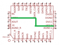
I also started to redesign es9038q2m board.
I will totaly split the supply so 5..6 or 7 regulators will be used.
I found one problem ...or not ...i want to splitt supply lines on both sides of dac and AVCC, but after disconnecting pin 12 VCC 3.3V the voltage is still present on that pin. Can be that it is connected with pin 27? in that case i can not use 2 different regulators for that 2 pins.
Can anybody test if dac plays normally if it is disconnected smd beard that is connected at that pin. I think it is not ok that 2 pins are supplied from both sides of dac with same supply line.
My idea... lt1085-5v for display and 5v pin that will feed i2s isolator. First 3,3v LDO for pin 27, second LDO 3,3V for clock, third regulator 3,3 LDO for DVCCpin 13, forth 3,3v LDO for VCC pin 12...if it is connected than not, fifth and sixth LDO for AVCCleft and AVCC right. All six are connected to TPS7A4700 5v preregulator that has best pulse noise, and low noise and qite ok current 1A. Output stage transformer output maybe with B1buffer at output, because i will connect it direct to power amp. Using digital volume.
Thank you
Attachments
looking on androa76 board V1.07 I see some ground traces between the i2s input lines I dont have on my v 1.04 board. would it be a good idea to stick some grounded copper film over the traces to shield them from top side? same might help on all digital (and analog) psu and signal paths?
One has to be careful with shielding and grounding. Adding a shield to something adds some capacitance that was not there before. There are mirror currents that flow in a shield if there is a return path somewhere for the mirror currents to circulate. If circulating in a return path, the currents can couple with other circuitry there.
That doesn't mean we shouldn't ground and shield of course, it just means that such things do not happen in isolation. If one shields when there was no need, it could create a new problem somewhere else.
The above kind of effects can be significant when dealing with sensitive circuitry or when power levels are high and circulating currents are large.
So, my perspective would be that experiments are probably okay, but if there is not a specific problem we are trying to fix or if an experiment does not produce a clearly beneficial result, then maybe better to stick with, or revert to the original circuit. Just could be the original designer had some good reason for doing what they did other than just to be cheap as possible.
There may be some exceptions to my above perspective, say if a designer was clearly trying to save money by skimping on quality components or not following well established practices for things like power bypassing in well understood circuits, etc., then it may not be unreasonable to decide there are problems based on simple inspection. However, if you notice a new problem soon thereafter, one of the first places to look would be at anything you touched or changed. I have seen cases where someone touched something they didn't even know they touched and it ended up being the source of a new problem. Just saying.
Last edited:
9028 Pro current requirements
Yes, I put an ES9028Pro on my Buffalo III | Dimdim's Blog
ES9028Pro power wows | Dimdim's Blog
op amps won't cut it for the 9028pro.
Yes, I put an ES9028Pro on my Buffalo III | Dimdim's Blog
ES9028Pro power wows | Dimdim's Blog
op amps won't cut it for the 9028pro.
Looks like TP has 3.6v dual regulator just for AVCC, and it's only $65. Yes, it is possible to run AVCC at 3.6v, but IIRC that's about as high as it is supposed to go.
Also looks like the 1.2v supply current for the 9028PRO increased almost 50% when the sample rate was increased from 44.1kHz to 384kHz. Not clear how high it would go if the sample rate were run at 768kHz, or if using the DoP or DSD modes.
Also looks like the 1.2v supply current for the 9028PRO increased almost 50% when the sample rate was increased from 44.1kHz to 384kHz. Not clear how high it would go if the sample rate were run at 768kHz, or if using the DoP or DSD modes.
Last edited:
9028 Pro current requirements
Yes, I put an ES9028Pro on my Buffalo III | Dimdim's Blog
ES9028Pro power wows | Dimdim's Blog
op amps won't cut it for the 9028pro.
one can alway boost an op amp with a transistor or with an IC buffer. however I agree, it makes more sense to make a decent reg. at the moment for me the question still is monolith or discrete. LDO implementation appears not so simple at all. as discussed elsewhere, surrounding component type and quality may matter even more than their nominal values, and boost the price of such circuit significantly. the discrete reg appears to be more appropriate at the moment, but I think I have to find a better voltage reference than TL431 (which btw internally is a shunt regulator). and more importantly find out the best way how to minimise load transition effects on the reg. for the latest I need first to measure them, what is a task itself.
Hi Mark, Spartacus already has mentioned (#1194) the TP's dual-reg. I am 100% agree with his remarks. Also, Russ White at TP discussed somewhere the choice of ADM7150 (why not use LT3042(5) at AVCCs). The DVDD also runs at higher voltage than 1.2V, it is in between 1.25-1.30 V. By the way, any toughts on 100R on the output of the DAC?
By the way, Twisted Pair, who have been developing ESS based DACs and peripheral parts since the ESS DACs first came on the market, currently use an ADM7150 based reg for their AVcc upgrade option. An op-amp based solution can also work well, but there will be the exact same issue, as well as other issues.
Last edited:
Yeah AVCC does not like 12V one bit. It smokes on 12V.Looks like TP has 3.6v dual regulator just for AVCC, and it's only $65. Yes, it is possible to run AVCC at 3.6v, but IIRC that's about as high as it is supposed to go.
Also looks like the 1.2v supply current for the 9028PRO increased almost 50% when the sample rate was increased from 44.1kHz to 384kHz. Not clear how high it would go if the sample rate were run at 768kHz, or if using the DoP or DSD modes.
janos_904, Thank you for the reference to Spartacus' post. I do recall seeing it now. Also, I agree about the best solution depending on the specifics of a particular case, etc.
In addition, ESS does specify voltage limits in the data sheets as do many manufacturers. As Dimdim mentions, it is not clear exactly what data in the ESS data sheets ESS is trying to protect, so most people with NDAs try to respect the terms of the agreement and not talk about details not made public by ESS. Unfortunately, legal issues can be complex and not always seem make sense unless particulars of existing law are well understood.
Regarding 100R on the output, I assume you are referring to a series resistor. Usually, a small series resistor on the output of an opamp driving an external output to a possibly unknown or incompletely defined load is a good idea. For one example, too much capacitance, say, from long cabling could potentially cause excess loop phase shift which could then result in opamp oscillation or other erroneous or sub-optimal circuit operation. Having some resistance in series with the output can help isolate the opamp from such effects.
one can alway boost an op amp with a transistor or with an IC buffer. however I agree, it makes more sense to make a decent reg. at the moment for me the question still is monolith or discrete. LDO implementation appears not so simple at all. as discussed elsewhere, surrounding component type and quality may matter even more than their nominal values, and boost the price of such circuit significantly. the discrete reg appears to be more appropriate at the moment, but I think I have to find a better voltage reference than TL431 (which btw internally is a shunt regulator). and more importantly find out the best way how to minimise load transition effects on the reg. for the latest I need first to measure them, what is a task itself.
This fully explains why the chinese ess pro DACs designs have changed from using ADP150s ( 150ma) (9018 and 9028 designs) to LT1963 (1500ma) for 9028 and 9038 designs.
In so doing they were also able to increase the rates on DSD. I was wondering why some designs were only capable of doing DSD 256 and some DSD512 with essentially the same chips....I think the regs were part of the reason now. Board designs carried over from 9018 designs were possibly current constrained. It also explains the need for those larger heatsinks on the newer boards.
Why not just configure a superreg for 3.3V? The design is there and it performs well and can carry the current required.
Last edited:
- Home
- Source & Line
- Digital Line Level
- ES9038Q2M Board