I can report on using a R (4R) on the raw output of the DAC. This is preliminary finding only, our THD+N went down -3db. We are doing more tests but it seems that this mod helps with a lower quality board .
would not 4R put the DAC in the voltage mode? but what about HF noise on the raw outputs? has someone tried to decouple them with some 100-150pF?
Freezebox, there is an offset on the output of the DAC that will keep the electrolyte biased.
what if AC Signal exceeds DC Offset? Than capacitor works in a negative range it is not built for, no?
Output impedance is some 750 ohms, and you'd want to be well above that for vout mode. 4 ohms extra input impedance doesn't do that. It's either playing with the distortion correction or stabilizing the output of the dac by providing a real component to the load impedance.
The rails also run between 0 and 3.3v, how do you plan on inverting?
The rails also run between 0 and 3.3v, how do you plan on inverting?
Also, it can help a lot to monitor your DAC progress if you have a very accurate headphone amp and quality headphones, or another accurate reproduction system. I could provide some information on my findings to date in that area and offer some suggestions if you would like.
Thank you for all your posts and offers here. I already did some changes on my V 1.04 es9038q2m board:
- add 2 polymer elco caps 2x 390uf to AVCC instead of orig. 100uF cap which gave a big improvement in bass performance
- feed seperate power to AVCC for both channels. one of it also supplies the 1,2V reg for DAC analog. This mod. improved harshness a little and made the sound less exciting in a positive way.
- removed DC caps (DAC still in voltage mode) and replaced opamp with descrete opamp with DC offset adjustment - no big improvement in SQ
- added polymer cap to tantalium cap for clock PSU (not sure about this effect as it was combined with AVCC mods)
- feed clean Sigma 11 power to 3,3V reg, eliminating 8V reg on board
next step would be a new clock (golden TCXO from ebay 100mHz, 0.1ppm - any experience about it?) with seperate reg. and a current Output stage.
I am thinking of taking the i/V Output of my es9028q2m board with 2x LM47920 for i/v and 2x47910 for SE Output. I have figured out its schematic and post it later here - it is different to the others I have seen here so far. Alternatively I would probably test madds1 mod on the board with 2,0V RMS and no DC Offset (maybe adjustable with variable R). How would you describe the Sound Change from voltage to current mode?
Last edited:
The clock needs to have low jitter at 10Hz offset. Most clocks are only specified down to 12kHz offset and work poorly for audio DACs. Only a few 100MHz oscillators in stock at Mouser could serve well. All of those are specified at 10Hz offset and all are described as "ultra-low jitter" in the data sheets. (Lower clock frequency is possible but limits maximum bitrate playback modes and may require non-disclosure agreement for info to configure DAC registers.)
Some possible clocks to look at:
Chrystek CCHD-575-100
Abracon ABLNO Series
Connor Winfield OH300-71003SV-100.0M
Connor Winfield OH100-71005SV-100.0M
Connor Winfield VBLD861-Series
Some would be harder or more involved to mount than others. They all cost more than $20 each. There are a very few considerably better 100MHz clocks but they start getting quite a bit more expensive.
Some notes: I went with the Chrystek which required some modification of the circuit board because is it a little bigger than the old clock. Removed old clock by first removing volume pot header from pcb, then using chip quik "cheater" solder on old clock. Still have to get original solder hot enough to melt in order for it to mix with chip quik, but can do that part one pin at a time. Didn't have to use any hot air or heat the pcb from below. Oscillator just popped off when I was adding chip quik to the last pin.
On the issue of clean power, besides regulation on the DAC pcb the incoming power quality can matter a lot. Some kinds of noise can be tricky to filter out and clean up. Examples might include HF noise from diode commutation in linear supplies, and broadband RF noise from switchers. For the latter, and in the absence of a spectrum analyzer, some idea can be gotten by using a portable shortwave radio at frequencies of a few MHz. Waving the antenna around the circuitry may show the presence of conducted and radiated EMI. If detected, steps should be taken to clean it up. Same goes for headphone amps. When going for very high SQ things like that can matter a lot. If nothing to measure with at all, the only alternative may be trying various supplies and see if any detectable difference in sound quality between them. Adding fast turn off rectifier diodes such as hexfreds to linear supplies and upgraded linear regulator ICs can help. Unfortunately, not so much in the way of good negative linear regulator ICs I know of.
Last edited:
Yes. The anti-jitter feature works by performing ASRC on data clocked in by some external source clock (the "transport" clock) so that the DAC chip itself only has to rely on its own local crystal clock (the "DAC" clock). That local crystal DAC clock is the one we are saying needs to be good. http://www.esstech.com/files/4614/4095/4305/about-jitter.pdf
Last edited:
CDS, I was thinking about what might happen here. It could be that it hacks into the distortion compensation mechanism inside the chip, which, without NDA and Sabre willing to share, remains a (tiny) black box.
I got somewhat better improvement, good to see you report something similar.
Sorry I meant to say that our THD+N got worst not better..so +3db (using 4R)
Sabre has on chip anti jitter circuitry as one of its selling points. Does mounting a better clock lead to measurable improvements?
I think that clocks are the most overlooked item in the chain . A good clock will have a profound impact on how you hear the music. I want to repeat that...clocks have a major impact on the perceived SQ .
However it will not necessarily appear in THD+N measurements .
With present board , a change in clock is important but in the end it will still be ASRC. The correct way of doing this will be syncronous (you need 2 clocks). Furthermore , a clock that feeds direct the DAC ic is not ideal , better to use a buffer that will have a much better rise and fall time (of course you need a buffer with low added phase noise and also that buffer needs clean power )
Phase noise , jitter , is meaningless without clean power.
Thought maybe a good idea to post pictures of my particular Chinese DAC in one consolidated place. They mostly show circuits pretty close to what ESS recommends.
Hi Mark,
I have another few newbie questions: What are the use of the resistors you soldered on the rca output?
Did you already test the I2C connect on the 1.06 board?
I tried to connect a small oled screen with no results. I guess I have to upload some software to access the data. Is that right?
Thank you
Attachments
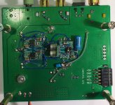

The resistors were put there before I decided to remove the output coupling capacitors. They were to make sure the caps could discharge if whatever the DAC board was connected to had coupling caps too, and no path to ground.
Regarding the I2C connection, I have looked at it. There is data constantly flowing between the microcontroller on the board and the DAC chip. I captured some of the data to look at and decoded it into hex instructions. It shows register addressing and data I/O with the DAC chip. Since I have not signed a non-disclosure with ESS at this point I am not privy to what the register contents are.
Regarding non-disclosure, I want to hold off on going that route for as long as possible so I can speak freely about modding the DAC boards. Also, I am still waiting for a bit more kit to arrive from China such as a low-cost USB to SPDIF adapter I hope to get working. Once I have done all I can without a non-disclosure agreement and assuming nobody who has one comes along to offer some programming assistance then I may see if I can get the confidential documentation.
The documentation would be needed for me to do the last bit of testing I would like to do with the SRC4392 and ES9038Q2M DAC. As cdgames alluded to, the DAC can be fed data using its clock as the I2S master and with jitter correction turned off. I think the SRC4392 probably ought to be able to work effectively in that mode if sufficient care is taken with the hardware interfacing and SRC4392 master clock (MCLK) quality.
If it was to improve the sound quality of my particular DAC as cdgames described, then I might have to see if I could make an acceptable closed-and-locked microcontroller code available for any DIYer's who would want to use it to set up the ES9038Q2M DAC board to work with an SRC4392 or some other slave mode I2S data source.
Last edited:
Sorry I meant to say that our THD+N got worst not better..so +3db (using 4R)
Was it after you optimized distortion through the 9038 registers, or before?
next step would be ...a current output stage.
I am thinking of taking the i/v output of my es9028q2m board with 2x LM47920 for i/v and 2x47910 for SE output. I have figured out its schematic and post it later here - it is different to the others I have seen here so far.
Here the schemata of this es9028q2m board Assembled ES9028 I2S input decoders ES9028Q2M mill board DAC balance output | eBay~-

It is different to ESS proposal regarding Vref and outputs from I/V to symmetry opamp is reverse in polarity. Does it make sense like this? Not yet tested to connect it to my es9038q2m DAC Output..any comments?
Last edited:
Was it after you optimized distortion through the 9038 registers, or before?
Thats an excellent question , I will have to check.
@freezebox, Regarding proposed schematic, why not connect non-inverting inputs of first two IV opamps to 1/2 AVCC? Also, if I read that correctly 10 ohms seems like a rather small output decoupling/current-limit resistor for the differential output stage. What load impedance do you anticipate it needing to drive?
Also, you might consider using those little Vishay SMT resistors rather than axial metal film. The resistors are more linear and some people think they sound better. If going for the best sound quality it's probably not unreasonable to try and see what you think or how your measurements look. The resistors are available in very tight tolerances for close gain matching of circuitry, and the 1/8 watt versions aren't too small to handle easily and can be soldered onto perf-board or whatever you want to use for prototyping.
Of course, it goes without saying to pay careful attention to power decoupling at ICs using 10uf tantalum in parallel with .01uf to .1uf Z7U ceramic or something like that. Film caps such as popular Wima can be used to provide low impedance at audio frequencies and up to 100kHz or so, but aren't so good at RF where opamps can oscillate. Okay to put them in parallel with other power filtering and decoupling caps if you find it improves sound quality. I just mention some of these things because they don't show up on schematics and I don't know what you may have in mind.
Lastly, I have been playing around recently with adhesive-backed copper foil to fabricate ground planes on prototype boards or sometimes when doing mods. You can order cheap rolls of it from ebay, or buy smaller amounts for shielding the internal wiring cavities in electric guitars. The foil is pretty thin, and joints should be soldered together, but I think it works a lot better than no ground plane at all. Helps lower return inductance for decoupling caps.
Last edited:
I agree that the non-inverting op-amp inputs should be connected to 1/2 AVCC. So add another 4k7 resistor to AVCC.
I would scale the components in the output stage, e.g. making the resistors 1/10'th the values and the capacitors 10x the values. This will reduce the noise considerably.
The 330 ohm resistors in the I/V stage could be changed to a higher value.
For the output resistor I would use 47 ohm.
For ceramic decoupling capacitors I would use X7R. The ones in the audio path should be NP0. Or film if you prefer that.
And yes, the polarity seems to be wrong.
Last edited:
Sabre has on chip anti jitter circuitry as one of its selling points. Does mounting a better clock lead to measurable improvements?
Nonetheless, a jtest on the stock implementation would be telling to determine need for a replacement clock. It's not uncommon for these crystals to be better than spec when fed with a stable supply.
Agree on lowering the impedance around the differential amp and connecting the non inverting to mid-rail.
Insofar the 330 resistors in the i/v, I think its a great place to think about target output volume and your system's gain structure. No point in excess gain here if you then need a huge downstream attenuation. Likewise getting as much gain as you need as early in the chain preserves snr.
MarkW4 and JensH,
Thanks a lot for your comments! This shown layout in post #594 I read out from my already existing es9028q2m board I linked to my post. I am planning to just use the i/v stage of this board and connect it to my es9038q2m DAC IC outputs. So I don´t want to build a complete new board or replace all components.
I will check again if I missed a connection of AVCC via 4K7 to the i/v Inputs when writing out the schematics. I think this is an important advise when connecting it to my other board - thanks! So should I remove the cap in parallel to the existing 4K7 resistor?
Regarding polarity change this is probably an error of the es9028 board design, so in this case the absolut polarity would be changed when using this i/v output, correct?
The output resistor on the board is only 10 Ohm, - I am not sure what is the Input impedance of my active crossover I connect the outputs to... but it worked fine with the es9028 DAC board only..
The opamp PS are all connected with ceramic 15uF caps to ground + 100uF elcos in parallel. I added 100nF wima film caps (MKS) from Vc+ to Vc-.
In case my plan works fine, I will think about your advices of replacing the resistors and caps to better ones and scale the values - thanks again for this!
Last edited:
One consideration with lowering resistor values around the differential amp, while it would reduce noise it also increases output loading on the opamp. Any load connected to the RCA output would further load the opamp. Not a worry insofar as the particular opamp used can drive the total load without producing undesired increased distortion. It is not uncommon for opamp distortion to increase as load current increases. Good to check the datasheet and try to balance requirements for low noise with low distortion. (side note: In general, distortion may also vary with maximum signal level, common mode input offset, etc. Curious readers may find some interesting discussion in the book, "The Art of Electronics." Given all sources of distortion, there may be a distortion budget to manage.)
Also, the IV input stages are already loaded with 300-ohm resistors. Decreasing resistors around differential amp may further load input stages.
In addition, it looks like the resistor values shown may be the same as those recommended by ESS. If so, it might make sense to try to figure out why they chose the values they did.
EDIT: Sorry for all the edits on this. Something about lowering the resistor values was giving me an uneasy feeling, but it took me awhile to think about it. That, and I just woke up.
Last edited:
- Home
- Source & Line
- Digital Line Level
- ES9038Q2M Board