Hi Cannonnica,
Now I have one more schematic to add to the mix.
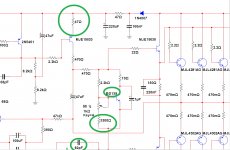
Aside from the things you noted in post #1878 I see these differences. You have a 1k pot across R5b. That makes me look at the two 47R resistors that replace D1 and D3. I sse that I have different brands in those two spots. This may account for the offset that I was seeing. I will replace those with identical (measured) resistors and see it that helps. If not I will install a pot like you did.
Also, on all other schematics R17 goes to ground. On yours it goes to C7 and essentially the input. Did you actually change that or is that a typo?
Just trying to get a final schematic put together before I do any more soldering.
Thanks.
Now I have one more schematic to add to the mix.
Aside from the things you noted in post #1878 I see these differences. You have a 1k pot across R5b. That makes me look at the two 47R resistors that replace D1 and D3. I sse that I have different brands in those two spots. This may account for the offset that I was seeing. I will replace those with identical (measured) resistors and see it that helps. If not I will install a pot like you did.
Also, on all other schematics R17 goes to ground. On yours it goes to C7 and essentially the input. Did you actually change that or is that a typo?
Just trying to get a final schematic put together before I do any more soldering.
Thanks.
OK I think I have found a couple mistakes on my boards the may have attributited to my problems. First, in post #1763Ranchu posted a schematic that showed R22 as 47R. I didn't notice that Carlos changed that to 10R in the following post. I believer the original value was 4R7 which is what it is in Canonnica's schematic above. Anyway, I have 47R in there and that may explain why my VAS is running too hot.
Secondly, when I was first populating the boards, I tried to use all of the resistors and diodes that I had in my parts drawers before I ordered parts so I didn't just continue to order parts I didn't need. Well I only had two 47R resistors so I put those in place of D1 on both boards. When the parts I ordered came in I put the new 47R resistors in place of D3. I just measured then and the resistors in D1 measure 46.R5 and the ones in D3 measure 47R3. Not sure yet but this may account for the high offset. I have a wedding to go to so I won't get a chance to test this until later. Just thought I would throw this out.
Blessing, Terry
OK, well I have made some headway. I replaced the two 47R resistors that replace D1 & D3 as they were not measuring the same. The offset is fine now. I had 47R in R22. I replaced that with the 4R7 shown in the original schematic. That fixed the problem with setting the bias but the VAS still runs pretty hot. Needs the big heatsink still. My house voltage is high today and the rails are +/- 77Vdc. I hooked up the scope and it now doesn't clip until 47Vac into an 8R load which is something like 275WRMS which is way louder than I will ever play it so that weird little sticking is not likely to be a problem.
The square wave still looks a little like the one in the picture above so I am going to try some of the fixes that Canonnica suggested. That picture is not of the amp clipping by the way. I has that funny shape right from the beginning.
I didn't play music through it yet as I don't have it bolted to the heatsink, only the angle. I made sure not to run it long enough to over heat.
I still have to replace the resistors in the other channel and then I will deal with the ground loop that seems to be there.
Blessings, Terry
Well...i gonna post the images here too.
Same amplifier...so..let's go.
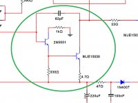
Schematic and the way to reduce VAS heat..also BD139 used into the bias control and thermal sensor (the VBE multiplier).... a standard schematic i have simulated once again few minutes ago.... nice and stable.
See the VAS resistor, the absence of decoupling capacitor there into the emitter...observe the 47 ohms resistors into the rails.... see the 22 ohms changed by 47 ohms in the VAS CCS... see the 82pf in the compensation (VAS).
Be happy....i am following your progress..from time to time i come to the computer to see if there's something new.
I use to go to sleep at 9 hours night...but tomorrow 4 AM i will be here again.
I use to see the forum making backup because they think no one are logged..... hehehehe...i am and i use to be waiting the back up to finish.
regards,
Carlos
Same amplifier...so..let's go.
Schematic and the way to reduce VAS heat..also BD139 used into the bias control and thermal sensor (the VBE multiplier).... a standard schematic i have simulated once again few minutes ago.... nice and stable.
See the VAS resistor, the absence of decoupling capacitor there into the emitter...observe the 47 ohms resistors into the rails.... see the 22 ohms changed by 47 ohms in the VAS CCS... see the 82pf in the compensation (VAS).
Be happy....i am following your progress..from time to time i come to the computer to see if there's something new.
I use to go to sleep at 9 hours night...but tomorrow 4 AM i will be here again.
I use to see the forum making backup because they think no one are logged..... hehehehe...i am and i use to be waiting the back up to finish.
regards,
Carlos
Attachments
Martin what did you get for your 8 ohm power output with the 45v tranformers ..?
You mean measured output power? I only have a 6 ohms resistor for load testing. I sustain 38.2V RMS before clipping (approx 240W RMS)
OK I'll try it.
Watch out about the BD139, the pinout is different. It's not a simple component swap on the board.
You have a 1k pot across R5b.
This is for setting the offset to zero. Once it's zeroed, I measure the effective resistor value across the pot and i put a fixed resistor of the closest value.
Also, on all other schematics R17 goes to ground. On yours it goes to C7 and essentially the input. Did you actually change that or is that a typo?
It goes to the lifted ground (R31) that you replaced by a jumper i think...
BD139 does not change sound...it is just better to adjust
Because if you use the resistors shown in the diagram...from base to emitter...the series of trimpot and a fixed resistor, then you will have small current into the output, less heat and nice operation.
Because of the gain, the MJXXXX is complicated to adjust, we do not have resistor values that match perfectly..or the current to each power transistor is too much big or too much small....we cannot use trimpot in the midway, we have to go to extreme..also it is harder to insulate...BD139 have a metal side and just a screw..have only to check if the screw make short with the colector...because screw goes to heatsink and this is ground...so..it is a short to ground..check this in advance to power your amplifier on..if the BD139 colector is shorted to ground (screw sometimes does that).
Replace the 22 ohms CCS resistor to 47 ohms to reduce the heat in the CCS transistor...i have checked and performance to 8 and 4 ohms is fine this way.
regards,
Carlos
Hi Terry-Hi Bonfis,
Yesterday I put a 1k2 in there and am able to adjust the bias at the 75V rails. However I am not too happy with the amount of offset an how dependent it seems to be on the temperature of the VAS transistors. I fashioned some large heatsinks and connected them. They are keeping the temperature down but still I see the offset rise as they warm up. I have the two transistors sharing the heatsink and I am now wondering if that is a mistake. Today I will try attaching separate heatsinks and see how they react to that. I still have about +40mv offset. I know that won't hurt anything but I'd still like to see it a little lower.
Blessings, Terry
I don't understand why the VAS temp would influence the offset voltage. My understanding is that offset is mainly dependent on the balance of the input pair. Any chance that that there is some other problem that is causing both the higher offset and the VAS heating?
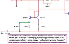
Here you have the reduction in the off set voltage
The ideas is to reduce the 100 ohms value...if this does not work, or work opposite way..then increase it to 120 and go reducing using the parallel resistor method.
Sometimes the bias in the threshold, when transistor goes conducting and cutting, produce off set variations...this happens because the capacitor you have in the VBE multiplier....it goes charging, this goes increasing voltage, then power transistors conducts and drain current..then the voltage drop and transistor cut once again...capacitor discharged now start all over again to charge.....increasing the stand by current often is the cure to the overflow.
Coupling thermally the differential transistors, touching one to the other, thermal grease and heatschrink tubes to keep them together also helps.
But damaged, leaky capacitors, inverted capacitors does the same..so.... check and replace capacitors...this happens a lot here...because junk capacitors..sometimes i found one or two with leakage... 1969 capacitors
regards,
Carlos
Attachments
Last edited:
Hi Terry-
I don't understand why the VAS temp would influence the offset voltage. My understanding is that offset is mainly dependent on the balance of the input pair. Any chance that that there is some other problem that is causing both the higher offset and the VAS heating?
I can only tell you what I see. Now that I have replaced the two 47R resistors with matched, the offset starts at -7mv and as the VAS heatsink warms it gradually swings to +7mv. I am just now sitting down to try the changes that Carlos has suggested. I will let you know how that works. My plan with the BD139 it to attach with wires and mount it on top of one of the output transistors. I'll let you know how that works for me.
Blessings, Terry
Very good Terry.... increase the CCS resistor from 22 ohms to 47 ohms
This may help a lot to control your VAS temperature..then tweak the off set
BD139 at the top of the power transistor works fine if your amplifier is overheating.
At the heatsink you gonna have better control of the temperature.
regards,
Carlos
This may help a lot to control your VAS temperature..then tweak the off set
BD139 at the top of the power transistor works fine if your amplifier is overheating.
At the heatsink you gonna have better control of the temperature.
regards,
Carlos
the change in the VAS affects the Vbe and Ib that it presents to the preceding stage.Hi Terry-
I don't understand why the VAS temp would influence the offset voltage. My understanding is that offset is mainly dependent on the balance of the input pair. Any chance that that there is some other problem that is causing both the higher offset and the VAS heating?
That effect is to throw the LTP pair into or out of balance, i.e. the output offset changes.
The LTP must be set up as close to exactly balanced as possible.
The other transistors should be adequately cooled to minimise the change in temperature.
the change in the VAS affects the Vbe and Ib that it presents to the preceding stage.
That effect is to throw the LTP pair into or out of balance, i.e. the output offset changes.
The LTP must be set up as close to exactly balanced as possible.
The other transistors should be adequately cooled to minimise the change in temperature.
Andrew thanks for that explanation. So I assume that this is an effect that a current mirror on the LTP cannot compensate for?
- Status
- Not open for further replies.
- Home
- Amplifiers
- Solid State
- Dx Blame MKIII-Hx - Builder's thread