I'm adding myself here to the general setup question. From the pictures you've posted Ian, I see the Si570 board being used.
- can the Dual XO Board be used as well? If yes, with which clock frequencies?
- which one would yield better results, Si570 or Dual XO with good clocks?
Thanks,
Abel
- can the Dual XO Board be used as well? If yes, with which clock frequencies?
- which one would yield better results, Si570 or Dual XO with good clocks?
Thanks,
Abel
I'm adding myself here to the general setup question. From the pictures you've posted Ian, I see the Si570 board being used.
- can the Dual XO Board be used as well? If yes, with which clock frequencies?
- which one would yield better results, Si570 or Dual XO with good clocks?
Thanks,
Abel
Abel and everyone else asking these questions. I agree there are some things that aren't immediately obvious on what configuration will suit your system(s). Especially considering the number of modules and flexibility that Ian works into his designs to make them as broadly applicable as possible.
Ian's said he's working on a pretty comprehensive user manual which I'd expect to cover most of these questions so I'd suggest holding off a little until Ian finishes that up. Going on experience with previous FIFO developments that Ian's taken on, user manuals and documentation will be around before it comes time to place actual orders.
Cheers,
Chris
Total 116
TV Man x 2
merlin el mago
rtd
jameshillj
erin x1 (or 2)
Nikola Krivorov x1
Rupor54
vitalica
analog_sa x 1
andrea_mori x 5
dsavitsk
tagheuer
hirez69 x 2
ccliu x 2
BDL
cddumat
regal x 2
zoran
Jogi
Zen(zenelectro) x 2
Buzzforb
SPWON
crobbins5421 X 2
marcus1 x1 (or 2)
casshan x 2
Dweeb99 X 2
jackw X 2
kazap X 2
danzup x 3
Giordano x2
Tony_T
Tubo x1
clivem x2
noizas x4
JoeyDD x2
skullaudio
dinos8746 x2
dvb-projekt
bisesik x2
guglielmope x1
Valeriano x1
mhgawel x1
av-trouvaille x 1 (or 2)
iloveswan x1
dtses
Flyboi X1
Lil' Knight x1 (or 2)
skippyboy x1
acccruz x1 (or 2)
WhiteBull x1
hksidney x 1
vts2006 x 3
JustBuildLspkAS.x3 &1 fifo kit finished for pcm1704 (ihave AD1862 ,pcm63,pcm1704)
54: PET-240 2 * TDA1541
TonyB
damohpi x1
iloveswan x 1
Joseph K x 2
mefistofelez x2 (pcm63P)
JLOP x1 (WaveIO, AD1865 NOS SRPP)
sceglar x1
4me2ctv x 1
tubesguy x 1
ctrange x 1
spm x 1
Joonas x1
Loboone x 1
flowerpot x 1
pavelal x 1
Steve Ha x 1
new2hifi x 1
Superdad x 1 (WaveIO, PCM1704K, discrete I/V)
Greg Stewart x 1
panther5429 x 1
supra x 3
Clsidxxl x 1
NATDBERG x 1
Uchi Deshi x 1
kvl x 1
palmito x 1
davej x 1
crowlie x 1
WhiteBull x1 (and one Dual XO Board, in case ones left)
nedi x 1
gonmar x 1
LuisMCP x 1
Hi Ian,
is it possible to use your I2S to PCM board to drive this DAC? http://www.dddac.com/documents/dddac1794_nos_ver30.pdf
The schematics of the actual board is here:
apoo
is it possible to use your I2S to PCM board to drive this DAC? http://www.dddac.com/documents/dddac1794_nos_ver30.pdf
The schematics of the actual board is here:
apoo
Total 118
TV Man x 2
merlin el mago
rtd
jameshillj
erin x1 (or 2)
Nikola Krivorov x1
Rupor54
vitalica
analog_sa x 1
andrea_mori x 5
dsavitsk
tagheuer
hirez69 x 2
ccliu x 2
BDL
cddumat
regal x 2
zoran
Jogi
Zen(zenelectro) x 2
Buzzforb
SPWON
crobbins5421 X 2
marcus1 x1 (or 2)
casshan x 2
Dweeb99 X 2
jackw X 2
kazap X 2
danzup x 3
Giordano x2
Tony_T
Tubo x1
clivem x2
noizas x4
JoeyDD x2
skullaudio
dinos8746 x2
dvb-projekt
bisesik x2
guglielmope x1
Valeriano x1
mhgawel x1
av-trouvaille x 1 (or 2)
iloveswan x1
dtses
Flyboi X1
Lil' Knight x1 (or 2)
skippyboy x1
acccruz x1 (or 2)
WhiteBull x1
hksidney x 1
vts2006 x 3
JustBuildLspkAS.x3 &1 fifo kit finished for pcm1704 (ihave AD1862 ,pcm63,pcm1704)
54: PET-240 2 * TDA1541
TonyB
damohpi x1
iloveswan x 1
Joseph K x 2
mefistofelez x2 (pcm63P)
JLOP x1 (WaveIO, AD1865 NOS SRPP)
sceglar x1
4me2ctv x 1
tubesguy x 1
ctrange x 1
spm x 1
Joonas x1
Loboone x 1
flowerpot x 1
pavelal x 1
Steve Ha x 1
new2hifi x 1
Superdad x 1 (WaveIO, PCM1704K, discrete I/V)
Greg Stewart x 1
panther5429 x 1
supra x 3
Clsidxxl x 1
NATDBERG x 1
Uchi Deshi x 1
kvl x 1
palmito x 1
davej x 1
crowlie x 1
WhiteBull x1 (and one Dual XO Board, in case ones left)
nedi x 1
gonmar x 1
LuisMCP x 1
chansiukwing x 2
Hi Ian,
is it possible to use your I2S to PCM board to drive this DAC? http://www.dddac.com/documents/dddac1794_nos_ver30.pdf
The schematics of the actual board is here:
apoo
I'm interested in this too! It would be great to have the option to drive the DDDAC1794 directly!
Abel and everyone else asking these questions. I agree there are some things that aren't immediately obvious on what configuration will suit your system(s). Especially considering the number of modules and flexibility that Ian works into his designs to make them as broadly applicable as possible.
Ian's said he's working on a pretty comprehensive user manual which I'd expect to cover most of these questions so I'd suggest holding off a little until Ian finishes that up. Going on experience with previous FIFO developments that Ian's taken on, user manuals and documentation will be around before it comes time to place actual orders.
Cheers,
Chris
Thank you Chris, will wait then ...
Hi Ian,
is it possible to use your I2S to PCM board to drive this DAC? http://www.dddac.com/documents/dddac1794_nos_ver30.pdf
The schematics of the actual board is here:
apoo
Hi apoo,
Nice project!
From the spec, PCM1794 is not a traditional R-2R DAC, and it accept right justified format which is not the 'PCM' format. So, I don't think you need this I2S to PCM converter.
It's very nice you run it at NOS mode
") .
.Ian
Last edited:
Gday Ian,
Just wondering if we use your adaptor to make it right justified then run into the FIFO, is that a possibility or is there an easier way I'm missing? The Amanero will output right justified I believe just havent had time to check, Doede also delays one channel by 32 cycles to make the signal equal in the time domain. any thoughts on this please?
Many Thanks for the efforts!
Drew.
Gday Ian,
Just wondering if we use your adaptor to make it right justified then run into the FIFO, is that a possibility or is there an easier way I'm missing? The Amanero will output right justified I believe just havent had time to check, Doede also delays one channel by 32 cycles to make the signal equal in the time domain. any thoughts on this please?
Many Thanks for the efforts!
Drew.
HI Drew,
FIFO can receive all formats and can output both I2S and 32bit left justified. I don't know if that is what you want.
Is that 32 bit delay for dual mono DAC configuration?
Regards,
Ian
Attachments
Do you want to skip the delay line from DDDAC 1794 main board?Hi Ian,
is it possible to use your I2S to PCM board to drive this DAC? http://www.dddac.com/documents/dddac1794_nos_ver30.pdf
The schematics of the actual board is here:
apoo
If no: you don't this I2S-PCM board.
Zsolt
Apparently my typing sucks......
The delay line as I understand it is so the left and right data arrive at the dac at the same time. reading the data sheet says the 1794 will take left or right justified, no idea how this is set and if it affects the NOS setup the Doede worked so hard for. im just wondering if the jitter induced by the 74HC chips is detrimental to the dac. if the FIFO can be setup to output right justified as a dual mono setup, but as I mentioned, in this regard I am a newbie and am not sure about any of this really. Happy to learn, just getting my head around it all....
Thanks,
Drew.
Let's try to touch bases...
First of all I assume you want to use the FIFO.
1. Doede's main board has I2S input, Ian's FIFO has I2S output... you can connect FIFO recloked output directly to Doede's main board input.
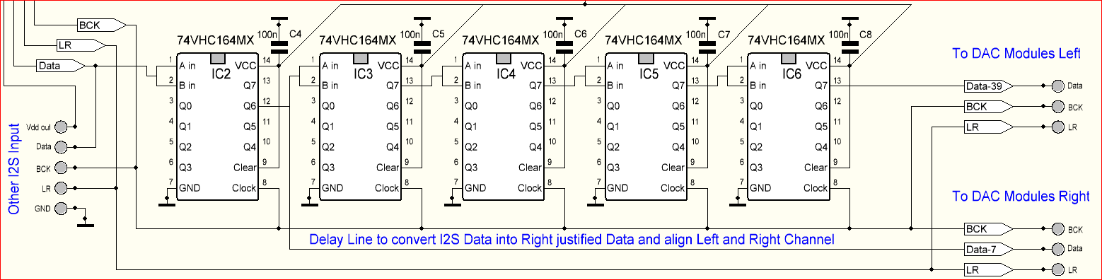
2. You want to skip the delay line from DDD1794 main board... you will need the FIFO + I2S-PCM converter board to convert I2S into MSB first, right-justified format and connect I2S-PCM output to [Data-39, BCK, LR] and [BCK, Data-7, LR] as DL -> Data-39, DR -> Data-7, LLLR -> LR, CLK -> BCK
You might want to ask Doede directly about point 2.
Zsolt
First of all I assume you want to use the FIFO.
1. Doede's main board has I2S input, Ian's FIFO has I2S output... you can connect FIFO recloked output directly to Doede's main board input.
2. You want to skip the delay line from DDD1794 main board... you will need the FIFO + I2S-PCM converter board to convert I2S into MSB first, right-justified format and connect I2S-PCM output to [Data-39, BCK, LR] and [BCK, Data-7, LR] as DL -> Data-39, DR -> Data-7, LLLR -> LR, CLK -> BCK
You might want to ask Doede directly about point 2.
Zsolt
Total 119
TV Man x 2
merlin el mago
rtd
jameshillj
erin x1 (or 2)
Nikola Krivorov x1
Rupor54
vitalica
analog_sa x 1
andrea_mori x 5
dsavitsk
tagheuer
hirez69 x 2
ccliu x 2
BDL
cddumat
regal x 2
zoran
Jogi
Zen(zenelectro) x 2
Buzzforb
SPWON
crobbins5421 X 2
marcus1 x1 (or 2)
casshan x 2
Dweeb99 X 2
jackw X 2
kazap X 2
danzup x 3
Giordano x2
Tony_T
Tubo x1
clivem x2
noizas x4
JoeyDD x2
skullaudio
dinos8746 x2
dvb-projekt
bisesik x2
guglielmope x1
Valeriano x1
mhgawel x1
av-trouvaille x 1 (or 2)
iloveswan x1
dtses
Flyboi X1
Lil' Knight x1 (or 2)
skippyboy x1
acccruz x1 (or 2)
WhiteBull x1
hksidney x 1
vts2006 x 3
JustBuildLspkAS.x3 &1 fifo kit finished for pcm1704 (ihave AD1862 ,pcm63,pcm1704)
54: PET-240 2 * TDA1541
TonyB
damohpi x1
iloveswan x 1
Joseph K x 2
mefistofelez x2 (pcm63P)
JLOP x1 (WaveIO, AD1865 NOS SRPP)
sceglar x1
4me2ctv x 1
tubesguy x 1
ctrange x 1
spm x 1
Joonas x1
Loboone x 1
flowerpot x 1
pavelal x 1
Steve Ha x 1
new2hifi x 1
Superdad x 1 (WaveIO, PCM1704K, discrete I/V)
Greg Stewart x 1
panther5429 x 1
supra x 3
Clsidxxl x 1
NATDBERG x 1
Uchi Deshi x 1
kvl x 1
palmito x 1
davej x 1
crowlie x 1
WhiteBull x1 (and one Dual XO Board, in case ones left)
nedi x 1
gonmar x 1
LuisMCP x 1
chansiukwing x 2
tassosk x 1
Hey Zsolt,
Appreciate the assist. Im figuring Doede has done the delay for a reason. The main reason I am thinking of straight from the fifo is to avoid the probable induced jitter from the 5 of 74VHC chips he uses for the delay. I have no idea if an FPGA could be capable of doing the delay before the fifo. The next thought I had was if delayed could two fifos be run off the one clock set so they run in time. the prob there would be the need to separate left data into one and right data the other. This is assuming I am understanding whether the FIFO does this already. I am just spitballing, so I realise this will have a bunch of issues conceptually so no need for a bunch of blokes to hang crap on an idea.
Understanding for me means being able to explain it to someone else and they understand. I am not at that point yet.
Really appreciate the assistance Zsolt, not trying to make you feel bad if I have.
Thanks,
Drew.
Let's try to touch bases...
2. You want to skip the delay line from DDD1794 main board... you will need the FIFO + I2S-PCM converter board to convert I2S into MSB first, right-justified format and connect I2S-PCM output to [Data-39, BCK, LR] and [BCK, Data-7, LR] as DL -> Data-39, DR -> Data-7, LLLR -> LR, CLK -> BCK
You might want to ask Doede directly about point 2.
Zsolt
Hi Zsolt,
am answering here for apoo and myself, we are working together on this projects.
Yes, the idea was to skip the DDDAC1794 mainboard by taking the signal straight from I2S to PCM board - if it would be a match.
From your quoted answer I deduct this is a straight match, since you mean that what Doede has named Data-39 and Data-7 is the same that comes out under DL and DR from the I2S to PCM board. Is my understanding correct?
Thanks,
Abel
The reason he has called it data 7 and 39 is sara 7 is the right channel and data 39 is the left. he delats the left by 32 cyxles which I am figuring is the number of "bits" or changes of state between the left and right channel. I dont remember why he delays rhe right channel, but from my understanding it is so the dac runs as dual mono, the left and right data is arriving at its chip at the same time to reduce any time smear I assume. But 32 cycles out of a 24MHz clock signal is not very long......
Yes, this is how I understand from Doede's document.From your quoted answer I deduct this is a straight match, since you mean that what Doede has named Data-39 and Data-7 is the same that comes out under DL and DR from the I2S to PCM board. Is my understanding correct?
But please check with him as well!
PCM1794 is configured for Digital filter bypass - Mono (see specs Table 2.)The reason he has called it data 7 and 39 is sara 7 is the right channel and data 39 is the left. he delats the left by 32 cyxles which I am figuring is the number of "bits" or changes of state between the left and right channel. I dont remember why he delays rhe right channel, but from my understanding it is so the dac runs as dual mono, the left and right data is arriving at its chip at the same time to reduce any time smear I assume. But 32 cycles out of a 24MHz clock signal is not very long......
He has to delay both channels in order to have 24bit right justified of both: delay right channel by 7 cycles and left by 39 cycles to have the LSB bit of both data channels clocked in when right channel's latch goes low.
31-7 = 24
63-39 = 24
(31 and 63 because I2S format has data delayed by 1 cycle).
Right-channels's I2S latch signal (LR) latches both L and R DACs.
Having reviewed how that works I'm 99% sure I2S-PCM board can be used to bypass Doede's delay line.
But why on earth use PCM1794 when you can use any good old R2R DAC with this I2S-PCM board?
Zsolt
Last edited:
- Home
- Source & Line
- Digital Line Level
- Drive NOS AD1865/62,PCM1704/02/63,TDA1541 from FIFO: Universal I2S-PCM driver board