same issue between WaveIO-I2S-to-PCM (good question how to connect them correctly) maybe remove the 7pin PH2.0 from the converter input and try solder u-fl connectors
Ian can be done Zsolt advice?
There is no such a commercial board, you have to design it and either etch it by yourself or send it to a PCB shop.Do you know where can I buy the adapter board with U.FL connectors?
If you haven't designed PCBs before this seems a very simple thing. You could try ExpressPCB (they provide you a design software as well) or find somebody who can do it for you.
Last edited:
Another alternative option would be to use isolated output of WaveIO. I would actually rather spend the time making a cable to suit the two boards than to make an additional adapter board to support u.fl for this interface at least. See Ian's post of interfacing WaveIO to the FIFO, same recommendations should apply here IMO.
For the output I would use JST PH -> bare wire. Since the pin out provides alternating grounds these can be twisted and will be still an improvement over the current arrangement, given that the DAC doesn't provide an impedence matched interface I think the benefit vs cost of the u.fl cables/sockets may be diminished.
For the output I would use JST PH -> bare wire. Since the pin out provides alternating grounds these can be twisted and will be still an improvement over the current arrangement, given that the DAC doesn't provide an impedence matched interface I think the benefit vs cost of the u.fl cables/sockets may be diminished.
For the output I would use JST PH -> bare wire. Since the pin out provides alternating grounds these can be twisted and will be still an improvement over the current arrangement, given that the DAC doesn't provide an impedence matched interface I think the benefit vs cost of the u.fl cables/sockets may be diminished.
I have tried it but the cables are very thick to connect to PCM1704
Attachments
Another alternative option would be to use isolated output of WaveIO. I would actually rather spend the time making a cable to suit the two boards than to make an additional adapter board to support u.fl for this interface at least. See Ian's post of interfacing WaveIO to the FIFO, same recommendations should apply here IMO.
For the output I would use JST PH -> bare wire. Since the pin out provides alternating grounds these can be twisted and will be still an improvement over the current arrangement, given that the DAC doesn't provide an impedence matched interface I think the benefit vs cost of the u.fl cables/sockets may be diminished.
Could you provide the link "See Ian's post of interfacing WaveIO to the FIFO"
TIA
Felipe
Could you provide the link "See Ian's post of interfacing WaveIO to the FIFO"
TIA
Felipe
http://www.diyaudio.com/forums/digi...ultimate-weapon-fight-jitter.html#post3218811

Thank you very much!!!!!!!!!!!!!!!
That's nice Zsolt
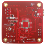
WaveIO Drive NOS
DT SD
LR WS
BC SCK
MC MCLK
TIA
Felipe
Still did'nt see how to connect it?
Still did'nt see how to connect it?
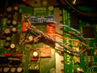
Use a female pin-header (or solder directly) the 7pin PH2.0 connector's cables to connect to the corresponding pins on WaveIO header.
You mapped the pins correctly:
WaveIO PCMconverter
DT SD
LR WS
BC SCK
MC MCLK - to connect MCLK to WaveIO pin header you probably have to skin/cut one end of the the u-fl cable
PCMconverter PH2.0 input has 4 grounds - connect all of them to the WaveIO pin header.
For the output:
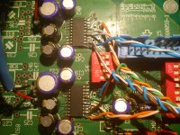
Use your existing soldered cables and twist ground cables around each line (CLK, LLLR, DR, DN) and solder them to PCM1704's PCB ground plane - e.g. to the ground pad of those unused electrolytic caps (C39...)
p.s.: post pics when you are done
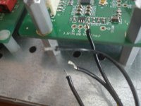
Attached pics prior to power the DAC.
Attachments
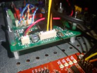
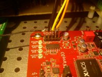
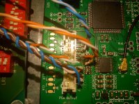
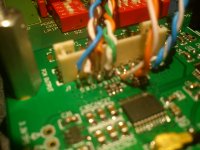
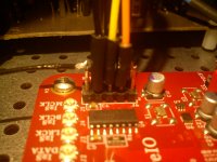
The cabling looks a bit better now.
1. Your WaveIO cabling seems incorrect according to this bottom image of WaveIO link . It seems you reversed all cables - e.g. MCLK should be on the other end
2. Please read/ask about WaveIO but I suppose at V+ pin you have to input some voltage for that part of the isolator - check this
- Measured and re-check that everything is connected and are no shorts among any cables/traces
- After everything lits up (you said you have a scope) - without connecting the converter board measure that you have the correct frequencies for WS, SCK and MCLK: e.g. 44.1Khz, 2.8224MHz, 22.5782Mhz or 176.4Khz, 11.2896Mhz, 22.5782Mhz
The cabling looks a bit better now.
1. Your WaveIO cabling seems incorrect according to this bottom image of WaveIO link . It seems you reversed all cables - e.g. MCLK should be on the other end
2. Please read/ask about WaveIO but I suppose at V+ pin you have to input some voltage for that part of the isolator - check this
- Measured and re-check that everything is connected and are no shorts among any cables/traces
- After everything lits up (you said you have a scope) - without connecting the converter board measure that you have the correct frequencies for WS, SCK and MCLK: e.g. 44.1Khz, 2.8224MHz, 22.5782Mhz or 176.4Khz, 11.2896Mhz, 22.5782Mhz
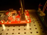
Awesome!
Oooops my fault, as you said I reversed all cables, thank you Zsolt.
merlin el mago,
Do you need single ended U.FL cables to improve signal quality? I can send you some.
Another thing is, all output signals of the daughter board work at 3.3V LVTTL logic level, I'm concerned about if your DAC can tolerance with this logic level when CLK frequency goes higher.
Regards,
Ian
- Home
- Source & Line
- Digital Line Level
- Drive NOS AD1865/62,PCM1704/02/63,TDA1541 from FIFO: Universal I2S-PCM driver board