Unless I do not understand how it works, I think that you are missing my point about I2S master/slave operation.
For example the PCM1794A acts as a I2S slave, the bit clock is an i/p.
The SPDIF receiver WM8804 is configured as a master, thus it generates the I2S bit clock, for the PCM1794A DAC, but as an example
The Si4735 is a I2S slave, its DCLK is also an input, what device in this case generates the bit clock? since you can't tie to I2S clock inputs together without a ref clock source.
As I said I'm not sure what tuner I am going to use yet. It's pretty far down on my to do list as it's pretty much useless where I live.
I do it the easy way and use a hot air recic station and solder paste, but it's pretty simple with an iron too. U3 on the board in post 39 is QFN. The board needs a wash, but that was done with an iron. The chip aligns itself better with hot air. It amazing how badly they can be misaligned with no issues.
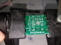
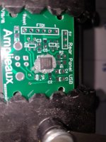
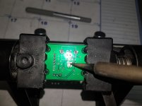
QFN Soldering
Here's a quick step by step install of a QFN IC. This is one of my rear panel USB to serial adapters.
First a quick alcohol wash. Next apply some liquid flux and low temp solder paste. Apply enough paste to ooze through the vias in the ground pad. As a general rule of thumb, apply about twice as much paste as it looks like you will need, this stuff really shrinks with heat. The liquid flux mixing with the paste makes it much more viscous, which helps too.
Install the IC and align it. Hold it in place and run around the circumference with an iron. Next reflow the pads a couple at a time and slide the iron away from the IC. Solder flows towards heat, this will draw excess solder out from under the IC and onto the external portion of the pad.
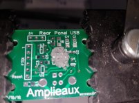
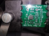
Flip the board and put the tip of the iron on one of the ground pad vias. Continue heating until all the solder in the vias is melted, and keep adding more until they are full (this is the heat sink for the IC).
Assemble rest of the parts, give it a bath and ready for testing. If there is any issues, reheat the IC. On these boards the QFN IC is usually fine, the issue is always that miserable little SC-70 USB filter.
Here's a quick step by step install of a QFN IC. This is one of my rear panel USB to serial adapters.
First a quick alcohol wash. Next apply some liquid flux and low temp solder paste. Apply enough paste to ooze through the vias in the ground pad. As a general rule of thumb, apply about twice as much paste as it looks like you will need, this stuff really shrinks with heat. The liquid flux mixing with the paste makes it much more viscous, which helps too.
Install the IC and align it. Hold it in place and run around the circumference with an iron. Next reflow the pads a couple at a time and slide the iron away from the IC. Solder flows towards heat, this will draw excess solder out from under the IC and onto the external portion of the pad.
Flip the board and put the tip of the iron on one of the ground pad vias. Continue heating until all the solder in the vias is melted, and keep adding more until they are full (this is the heat sink for the IC).
Assemble rest of the parts, give it a bath and ready for testing. If there is any issues, reheat the IC. On these boards the QFN IC is usually fine, the issue is always that miserable little SC-70 USB filter.
Attachments
Last edited:
how do these "hot air" not blow the components off the PCB?
As Jeff mentioned, the solder paste is pretty sticky out of the tube. Having said that, on a few instances I've managed to dislodge small components trying to solder down adjacent components...
") specially when I've set the hot air pressure too high.
specially when I've set the hot air pressure too high.Seen videos on youtube where folks cover some of the other components with Kapton tape, so nothing get's blown away or dislodged.
This looks like a really cool project!
+1
Last edited:
To add, the hot air machine has a air volume and temp control. There are also a number of different nozzles to use.
Jeff,
I was thinking about your hot chip issue for the PCM1794A app note example. One solution, a cheap one, is to parallel one or more opamps, in different pkgs that is, that way the o/p I is shared, thus heat is distributed across more devices. The expensive solution is to use a dedicated buffer such as the LME49600 device specifically designed for this purpose.
To add, the hot air machine has a air volume and temp control. There are also a number of different nozzles to use.
Jeff,
I was thinking about your hot chip issue for the PCM1794A app note example. One solution, a cheap one, is to parallel one or more opamps, in different pkgs that is, that way the o/p I is shared, thus heat is distributed across more devices. The expensive solution is to use a dedicated buffer such as the LME49600 device specifically designed for this purpose.
We're going to drop the opamps and use the jFET-based I/V converters
Anticipating to see what you come up with, good luckWe're going to drop the opamps and use the jFET-based I/V converters
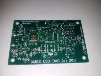
This web site provides some additional info on the PCM1794A
H-DAC – High performance 192 kHz / 24-bit DAC with addon options – nihtila.com
H-DAC – High performance 192 kHz / 24-bit DAC with addon options – nihtila.com
Perhaps I’m in the minority, but for me a full-featured preamp means mm / Mc Phono capability.
Any chance a simple Phono pre could be integrated into this design, even as an add on?
That would make this a perfect project for me.
Thanks for all your efforts either way. Looks to be shaping up well.
Any chance a simple Phono pre could be integrated into this design, even as an add on?
That would make this a perfect project for me.
Thanks for all your efforts either way. Looks to be shaping up well.
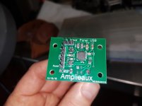
Hi Thimios. Things have been very busy here for the last couple months so I haven't gotten much of anything done. I have a new USB audio design ready for assembly and testing, but haven't had a chance to assemble it yet. I also haven't had a chance to put together a package for you either, I hope to do that today.
Hi Thimios. Things have been very busy here for the last couple months so I haven't gotten much of anything done. I have a new USB audio design ready for assembly and testing, but haven't had a chance to assemble it yet. I also haven't had a chance to put together a package for you either, I hope to do that today.
I hope the reason is the Christmas Holidays
Happy new Year!
- Home
- Source & Line
- Analog Line Level
- DIY Full Featured Preamp