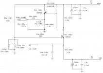
for your needs - you need to decrease sum current for regs to - say ~ 60mA max ( increase R1 in both regs to 10 ohms)
there is no need for more of that , if active stage is drawing 20mA
that way - roughly -overall consumption per channel is 60mA x Vdc = 60mA x 1,41 x 30V x2
regarding needed amplitude of output signal
considering that current output of PCM for full blast is +/-1.2mA - just divide your needed p-p amplitude with 2,4mA and you'll get value for R6
this way ( with R6 1K5) , you'll have 3V6pp on output
if you're going to use set of regs for both channels - go for 100mA as programmed current ; in that case R1's must be around 6R5
Last edited:

You should raise R2a's value a little bit unless you can accept around 1Vrms output. If you raise R2a's value, you need to change source resistors value accordingly too.
About Mosfet match, it's easy to get a 1% Vgs matched pair from same production batch.
@ZM
So don't need to change R2 as Iloveswan suggested & he do bad calculations 1Vrms instead 1.8Vrms?
Last edited:

@ZM
So don't need to change R2 as Iloveswan suggested & he do bad calculations 1Vrms instead 1.8Vrms?
Correct. you should change R6 not R2... sorry for typo...
I think that I have to reverse the polarity of lytic C1, the schematic is wrong right?
Please help
Attachments
Hi,
Didn't check the datasheet of the chip for specs but if it wants 0 volts at it's output you're doing fine. the dac will have a compliance range for dc offset at it's output and your offset is very very low. but check again after connecting to the dac. check the datasheet of the dac for it's output compliance.
regards
joris
- Status
- This old topic is closed. If you want to reopen this topic, contact a moderator using the "Report Post" button.
- Home
- Amplifiers
- Pass Labs
- DIY D1 I/V STAGE