this is hilarious...Skin-effect adds here the distortions and compression.
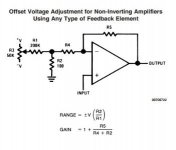
This is what I have used very successfully for offset trim. It limits the current through the pot wiper which is important. The resistor in series with the wiper should be adjusted to the largest that will accomodate worst case offset differential between the two fets.
The pot needs to be a good one. I used vishay foil but those are $$$. Carbon would not be good for this. Possibly a wirewound would be the best reasonable but cermet may be as good.
I have also found that a stable thermal housing and reaching operating temperature is important before attempting to adjust.
I have also found that in some cases the lowest distortion is not at the lowest DC offset of the amplifier. usually this is at the -130 dBC distortion levels or lower.
Thank you Martin.... This might be a good solution.
What do you think of this other idea ?
Explanation here: EPOT Applications: Offset Adjustment in Op-Amp Circu - Maxim
Attachments
Indeed! Probably thinks that the skin effect is worse with thin conductors. Duh! Look it up.this is hilarious...
Thank you Martin.... This might be a good solution.
What do you think of this other idea ?
Explanation here: EPOT Applications: Offset Adjustment in Op-Amp Circu - Maxim
Its a common solution, especially for opamps with no offset trim capability. It does require a stable external supply because the supply is the source of the correction. It can also inject noise etc if its not well managed. The circuit I use is also low noise and independent of external stuff. It would be interesting to check Vgs for a set drain current vs Vds. That has not been an issue in cascoded circuits for me since Vds is essentially fixed. I think internal adjustment of the actual offset would be best, especially if you are starting with closely matched Jfets. BTW I use depletion mode MOSfets for the cascode transistors these days. They work well.
Its a common solution, especially for opamps with no offset trim capability. It does require a stable external supply because the supply is the source of the correction. It can also inject noise etc if its not well managed. The circuit I use is also low noise and independent of external stuff. It would be interesting to check Vgs for a set drain current vs Vds. That has not been an issue in cascoded circuits for me since Vds is essentially fixed. I think internal adjustment of the actual offset would be best, especially if you are starting with closely matched Jfets. BTW I use depletion mode MOSfets for the cascode transistors these days. They work well.
Hi, I moved my questions here: https://www.diyaudio.com/forums/analog-line-level/349442-discrete-opamp-offset-trim.html#post6080225
Please keep an eye on the evolutions
")
Well, I don't know what I mean, Richard, except that to remove active parts from my example schematic would compromise it, somewhat. However, many here would add 10 more active devices in the follower stage, etc. I do shake my head at that.
By the way, this design would not need a servo if the gain were reduced to headphone levels, if that bothers you. '-) Just use a monolithic dual fet at the input.
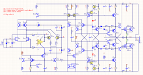
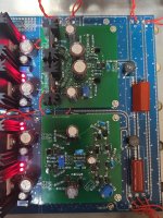
Ive gone and built this circuit for my modular preamp revealed in the photo. The preamp is a dual mono design, error correction ic regulators, ground plane/star ground mix, even vias fencing utilized and yes those are shielded input caps, haha.
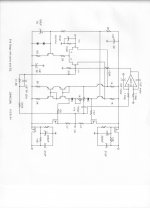
As for the module of john curl's circuit its the best out of dozen or so designs ive tried. For the jfet j309s were used, irf610/9610 output and 15v +/- supply. Gain is set for 3 and ive omitted the servo and the cmx. The circuit sounds very mellow and coherent and extremely clean. Its almost perfect except that the bass is kinda lose and slow. And thats the problem i want to figure out.
Should i have used latfet and with higher bias?
Should i add driver transistors?
And what should the value for the unmarked resistor on the far left be? (I set it at 3k for now)
Also any readily avail jfets that might be better choice than my 309s? (I should thermal couple them i know)
Attachments
Last edited:
LH0033 schematic is in its datasheet, attached below.
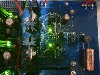
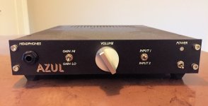
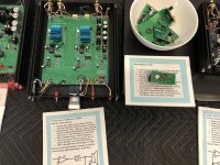
I demonstrated a DIY project called Azul at Burning Amp 2019. It was a headphone amp that used a composite topology: opamp plus high current buffer, enclosed in a single negative feedback loop. The high current buffer was an LH0033. Ti Kan photographed many of the Burning Amp exhibits and demos; his picture #19 is attached below.
The LH0033's have blue anodized heatsinks attached to their lid by thermal tape. To the right is a bowl full of "LH0033 emulators" which I plugged in during debug, because when something goes wrong during bring-up or testing, I'd rather destroy an emulator made of modern parts, than an expensive and hard-to-replace LH0033.
_
_
Attachments
Thanks Mark,
I have the datasheet for LH0033 and I figured the schematic was a conceptual one, but nice to know it is not!
I know EUVL has cloned it in SMD for Xen (Zen) but I have never gotten around to copying his work.
Then I happened upon a dozen LH0041 and my curiosity was piqued again
I have the datasheet for LH0033 and I figured the schematic was a conceptual one, but nice to know it is not!
I know EUVL has cloned it in SMD for Xen (Zen) but I have never gotten around to copying his work
.Then I happened upon a dozen LH0041 and my curiosity was piqued again
The LH0033 (especially the discrete version) has the advantage that it allows you to add a Sziklai booster to give a lot more Class A current at low distortion.
http://xen-audio.com/documents/xen-zgf/ZGF Desktop Description V1.pdf
Patrick
http://xen-audio.com/documents/xen-zgf/ZGF Desktop Description V1.pdf
Patrick
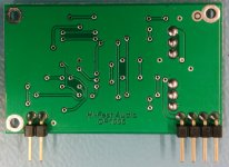
Worlds first?
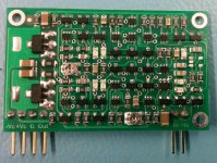
Scott wurcers opamp1 in thru hole.
Considering this was the hardest circuit for me to try out so far im surprised it works on the first try and works flawlessly. Stable bias and minimal dc drift.
Compared to the mini vssa (the module next to it) which is my reference at the moment it almost sounds the same which is to say it almost sounds like nothing at all. Vssa has a bit of edge in smoothness but swa1 has more pleasant treble.
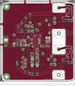
The layout is terrible, i know. I referenced it from how the original schematic is drawn and being such it has loong feedback traces from the input block to the output.
Would like your help on how to refine the layout. But so far, this one is a winner 😁😁
Scott wurcers opamp1 in thru hole.
Considering this was the hardest circuit for me to try out so far im surprised it works on the first try and works flawlessly. Stable bias and minimal dc drift.
Compared to the mini vssa (the module next to it) which is my reference at the moment it almost sounds the same which is to say it almost sounds like nothing at all. Vssa has a bit of edge in smoothness but swa1 has more pleasant treble.
The layout is terrible, i know. I referenced it from how the original schematic is drawn and being such it has loong feedback traces from the input block to the output.
Would like your help on how to refine the layout. But so far, this one is a winner 😁😁
Attachments
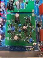
Also i stopped throwing ground planes down on all my layouts. If its ill adviced doing so for opamps because the parasitic capacitance can be clearly heard when u couple the chip to the ground plane why would this not be the same for a discrete circuit which is in the end basically a big spread out opamp?
Being costly and hard to get seems to be THE requirement for audiophile parts.I demonstrated a DIY project called Azul at Burning Amp 2019. It was a headphone amp that used a composite topology: opamp plus high current buffer, enclosed in a single negative feedback loop. The high current buffer was an LH0033. Ti Kan photographed many of the Burning Amp exhibits and demos; his picture #19 is attached below.
The LH0033's have blue anodized heatsinks attached to their lid by thermal tape. To the right is a bowl full of "LH0033 emulators" which I plugged in during debug, because when something goes wrong during bring-up or testing, I'd rather destroy an emulator made of modern parts, than an expensive and hard-to-replace LH0033.
We had the LH00* by the pound in our ultrasonics test gear for nuclear power plants.
Cost was no matter for testing the inner steel enclosure of reactors. ( "For each day earlier
done with your testing, you may contaminate a PDP11, we don't care")
The LH00* were designed out a week after Comlinear rolled out their first CFBs.
Never looked back.
I think I have still some boards with them in the basement.
Gerhard
- Home
- Source & Line
- Analog Line Level
- Discrete Opamp Open Design