Thanks much. I have a much earlier version of the manual. I'll see if I can note the changes.
2SC2240GR
NPN- Beta = 330 @5mA
noise at 3mA =
2nv 2.8 .7 .65 .6nv
THx-RNMarsh
Hi Richard,
Have you ran out of transistors to test?

No, not yet. Just been busy doing other things, recently. Eventually, I'll get to measuring some fet's also.
What is on the top of your list to test?
-RM
I have many 2SC1845 and 2SA992. Have you test them?
2nv 2.8 .7 .65 .6nv
2sc2240 looks very good, in spite of the 1/f knee higher than 100 Hz. It's long been a favourite of mine, including the SMD 2sc3324 avatar.
My wish list would include:
2sc1845/2sa992
2sc1815/2sa1015
N-channel JFETs:
2sk209
bf862
2n4393
2n4416
j310
I've used the last 3 as upper-cascode elements, and it's worth checking if they're also good as lower-cascode, i.e. common-source elements.
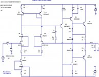
Here's a pic of the latest prototype of the FET990/LF06, with a modification to the output stage to bias it as a Class-A push-pull with a stage current of around 10 mA. LTP consists of 2SK209-BL cascoded by MMBF4416, VAS is FJV992 (thanks to Dmitri for the samples) with Icq of around 1.5 mA, all resistors are micro-MELFs (mostly Beyschlag thin-film), and all capacitors are C0G or stacked PPS.
It's running a bit warmer than I'd ideally like, with a total quiescent current of around 15 mA/opamp, but the audible sonics are noticeably better than the previous LF06 prototypes with Class-AB biasing - dark and detailed, with excellent dynamics and definition. I'm using it as the reference opamp for the I/V stage of my Marantz CD4000 (which has a bunch of other mods), with +/- 12V rails.
Edit: I omitted the evil VAS clamp diode in this prototype, with no audible issues - the moderately high rails of +/- 12V, along with a max output amplitude of around 2.8V in the I/V stage, should ensure that the VAS stays comfortably out of saturation.
Attachments
Last edited:
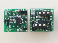
What an interesting off-board connector! 6 pins, dual inline, with an offset. Congratulations for "thinking outside the box" .
A little 99% isopropyl alcohol and a toothbrush will clean off the excess flux from that left hand picture. (Amazon sales page).
A little 99% isopropyl alcohol and a toothbrush will clean off the excess flux from that left hand picture. (Amazon sales page).
Thanks, I'll clean the debris off, and maybe also reflow some of the joints to improve the finish - I was busy listening to it for the last 2 days, so no time for cosmetics.
Pins 1 and 5 (typically offset pins) have been omitted on the assumption that the LTP will be matched for Vgs - this gives some additional space for parts placement, on both sides. The pinout is otherwise stock DIP8 single.
Pins 1 and 5 (typically offset pins) have been omitted on the assumption that the LTP will be matched for Vgs - this gives some additional space for parts placement, on both sides. The pinout is otherwise stock DIP8 single.
Here are the schematics of two variants of the output stage.
a)The first one is the Class-A push-pull in the picture a few posts earlier. It works and has excellent audible sonics at an output stage current of around 10 mA.
b) the second one uses an idea from Ken Peter to perform quadratic Schottky-commutated crossover. It's only in simulation at the moment, but is comparable to the Class-A topology above at around half the output-stage current (say about 5 mA). H2 is higher, but H3 is lower by about 3-5 dB. In practice, there will be some issues in obtaining predictable output stage quiescent current.
I'll try to kludge together the second one using a pair of the existing LF06 boards - no timeline at the moment.
Attachments
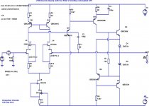
10mA of output stage current results in Vre of 270mV
Why operate at such a high Vre?
What about using Re=2r7 @ 10mA and then the stage operates in ClassA upto ~20mApk AND operates in optimal ClassAB for exceptional Iout exceeding 20mApk.
Are J5 & J7 the same device?
What about using a higher gm device for J5
Then you can have Vdsj5 >> Vpj5
Why operate at such a high Vre?
What about using Re=2r7 @ 10mA and then the stage operates in ClassA upto ~20mApk AND operates in optimal ClassAB for exceptional Iout exceeding 20mApk.
Are J5 & J7 the same device?
What about using a higher gm device for J5
Then you can have Vdsj5 >> Vpj5
Last edited:
What about using Re=2r7 @ 10mA and then the stage operates in ClassA upto ~20mApk AND operates in optimal ClassAB for exceptional Iout exceeding 20mApk.
If smaller emitter ballast resistors are used, then the diode chain has to have lower forward drop (maybe just one diode, or 2 Schottkys instead). It can be done, but Icq then becomes very twitchy and sensitive to ambient temperature.
Are J5 & J7 the same device?
What about using a higher gm device for J5
Then you can have Vdsj5 >> Vpj5
I had MMBF4393 and SST310 in earlier prototypes. It probably doesn't matter too much, though I'd probably want reasonably high Vgs (say 1..1.5V) across the current-setting resistor to maintain bias stability. For the lower JFET in the CCS, MMBF4416 fits the bill nicely, and so does MMBF102 (which however has a Vdg max of 25V, so an upper cascode is mandatory if we want to use standard +/- 15V rails).
Last edited:
I don't understand the operation of the quadratic law operation.
I have disputed it in another Thread without the knowledge to back up my intuition.
It seems to work in simulation, though I need to simulate it extensively in corner cases like overload and high swings. Ken Peter's intuition is fundamentally brilliant - it has a more desirable distortion profile (higher H2, lower H3) than just about any other Class-AB commutation mechanism, other things being equal.
Last edited:
bf862
j310
I've used the last 3 as upper-cascode elements, and it's worth checking if they're also good as lower-cascode, i.e. common-source elements.
Both had Quantech measurements in my Linear Audio article, I would watch out for high Ib at high voltage on the BF862 but its noise was exemplary.
... watch out for high Ib at high voltage on the BF862 but its noise was exemplary.
Thanks Scott, will check it out. It will be cascoded, so Vds is not a big concern.
... it has a more desirable distortion profile (higher H2, lower H3) than just about any other Class-AB commutation mechanism, other things being equal.
A place-holder link to the original posting with the Schottky-switched topology:
http://www.diyaudio.com/forums/soli...r-non-switching-need-revival.html#post2147462
(There are earlier references to using diodes (including Schottkys) to shunt or replace the emitter ballast resistors, but the intent in most of those cases seems to have been to limit power dissipation in the emitter ballasts. This is the first posting I've found where it has specifically been described as a crossover distortion-reduction mechanism.)
- Home
- Source & Line
- Analog Line Level
- Discrete Opamp Open Design