The signal current of the VAS is dependant of R9, right? So if I keep the current high enough it shouldn't pose a problem I think.
Not entirely. R9 accomplishes several things. Of course number one is that it provides the power supply voltage to the collector. It also sets the collector voltage based on the collector current which is in turn set by the sum of the input bias and the signal voltage. If you use an emitter resistor then R9 and the emitter resistor will set the voltage gain of the stage. As an aside I would recommend that you use an emitter resistor (you could bypass some of it) in order to control the open loop gain of the VAS.
The collector signal current (in the absence of any feedback) will be hfe times the input signal current. This collector signal current will be divided between R9 and the actual load so it is true that the output impedence (largely determined by R9) of the VAS will affect the output signal current but that is not sufficient to insure adequate current.
The transistor needs to be able to supply this current without exceeding its current and power ratings as well. So if you need say 500mA to drive the output stage a VAS device with max Ic of 200mA won't work. I think a common rule of thumb is to have the bias current in the VAS at least ten times the required current drive for the output stage to avoid loading down the VAS too much.
So there is a lot of interaction going on here. The current available to the output will depend on the current supplied by the transistor and the value of R9. But the current supplied by the transistor is determined by the forward current gain of the transistor and the input current and the impedence of the transistor itself. However the input current is determined by the input signal voltage and the impedence of the transistor and the bias network. But the input signal voltage is affected by the output impedence of the preamp and the input impedence of your circuit. So there factors all along the way that will affect the amount of drive current that you can supply and of course the physical limitations of the transistor can not be exceeded either.
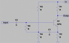
Your bootstrap circuit appears to be wrong also. See the attached bootstrap circuit. The input signal should not pass through the bootstrapped resistor as your drawing shows. The input signal goes directly to the base of the transistor and the bootstrap resistor (R5 in my drawing) acts to "insulate" the bias network from the input signal.
The voltage across the emitter resistor (R2) follows the input voltage (approximately) as in an emitter follower. The bootstrap capacitor (C1) applies the AC componant of this voltage to one side of R5 while the input applies an AC signal that is essentially the same to the other side of R5. So for the AC componant we have approximately a constant current and thus nearly infinite impedence.
So this configuration allows R5 to "pull it self up by its bootstraps" so that its effective AC impedence is much higher than its actual value. Since this very high impedence swamps out the voltage divider's impedence and is the only other impedence in parallel with the impedence of the transistor's base the total input impedence becomes essentially equal to the impedence at the base of the transistor. I don't think this will work as well without an emitter resistor because the emitter resistor raises the input impedence of the circuit. The input impedence is 1+hfe times the sum of the impedence of the base emitter junction and the emitter resistor.
I am not sure what part of the ESL site you were looking at but I do note that the bootstrap current source that he uses is a slightly different application of the same principle. He is using bootstraping to provide the equivilent of an active collector load without the actual active device. In the bootstrap bias we use the same technique to increase the input impedence to stage. Same idea, different application. Does he also get into the use of bootstrapping in the input somewhere else on his site?
I saw the schematic of a guy who posted it to ask for comments on his class A design, and when I compared it to my own design I saw that the imput capacitor C5 could be omitted. However, if for some reason a DC would be introduced I think it could reduce the effeciëncy of the VAS and since efficiëncy is already low I desided to keep it.
Good choice IMO. Why allow a failure in the pre-amp to take out your power amp?

By proposing the feedback capacitor I realize that this is POSITIVE feedback, so the increased signal current would increase the output which increases again the signal current ...
I will leave it to better minds than mine to analyze this but it looks suspicious to me. I haven't run it through a simulation (BTW I recomend downloading the free LTspice so that you can run your circuit ideas on the computer before commiting it to the breadboard) but It seems to me that you are asking for trouble with this kind of arrangement. However without an emitter resistor in the output stage I don't see that there will be much signal to feed back unless I am missing something. Why would the current have any reason to go through the capacitor and the imput impedence of the output stage when it can just go straight to ground?
According to hFE, a transistor amplifies current. By using a resistor network you can also amplify voltage, but I thought a trans. remains essentially a current amplifier. I think you mean that by using the two power devices, the one for the VAS would be overkill, but in this configuration isn't it supposed to act as a quickly varying resistance and thereby varying the voltage from the voltage divider network?
Actually there is debate about this point. I have recently read some materials that have pretty well convinced me that a BJT is a transconductance amplifier like tubes or FETs. The relationship of Vbe to Ic seems to be much more constant and predictible than hfe. You will note that hfe varies quite a bit WRT temperature, current and between different transistors of the same type.
But, that aside, yes using a power transistor is overkill in the current department but it also may be sub optimal based on other parameters. I could be entirely wrong but it seems likely that the design decisions which allow for high current operation might be quite different from those made for a device to be used in a low current voltage amplification stage.
When I say optimized for voltage amplification I am indeed talking about the entire stage design not the manner in which the device itself operates.