That circuit senses the output in parallel and provides the feedback in series with the input, series shunt feedback.
When responding to a change there will be current flowing from the emitter, this is the same current that goes into the TIS, current on demand (CFA). The gain/feedback makes this error current go to zero.
Lower the feedback resistor values (keeping ratio the same) and you will get more current for a given change.
Thanks
-Antonio
Yes, you can also analyze it as the difference in voltage (error voltage) between the inverting and non inverting inputs which appear across the transistor base and emitter. The error voltage gives rise to a current output which appears at the collector, much like the action of an LTP.
So, it's not entirely clear cut
Mmmm. On th otherhsnd, maybe it's CFA after all . . .
So, it's not entirely clear cut
Mmmm. On th otherhsnd, maybe it's CFA after all . . .
Yes, I agree they really aren't that different. The LTP has an error current (the difference between the two emitters) flowing through the collectors, though this error current is limited to the LTP bias current. The CFA allows one to adjust this error current (and bandwidth) by the impedance of the ground side resistor.
Thanks
-Antonio
Thanks
-Antonio
Gentlemen, here is a simple explanation of the principles and differences between the two topologies, it was posted in another thread but it covers the subject perfectly.
http://www.ti.com/lit/an/slva051/slva051.pdf
http://www.ti.com/lit/an/slva051/slva051.pdf
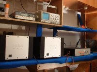
I finally got both monoblocks fitted with the new face plates. Took a picture of it too ") . The thing you see on the far right is my preamp. That's another project that earned its place on my system a few years ago and its going to be the next one to get a decent front panel. Its an implementation of Walt Jung's composite amp with the AD811/AD744 combo, so the whole system gives me a very wide bandwidth from preamp input onwards.
. The thing you see on the far right is my preamp. That's another project that earned its place on my system a few years ago and its going to be the next one to get a decent front panel. Its an implementation of Walt Jung's composite amp with the AD811/AD744 combo, so the whole system gives me a very wide bandwidth from preamp input onwards.
The preamp is on the bench also because I've swapped the volume pot from an Alps to a TKD one. I hooked up the system to make sure everything worked before taking it back up. Even when driving cheap speakers the hallmark of this system (detail) is immediately apparent. Love it.
So now its back to the drawing board for the preamp front. This time its a bit more than just an aluminum plate. Its also going to have some push buttons to select input, high bias and turn the monos on/off together with an input indicator. All driven by some pic I manage to find on the bin. I'll be taking pics along the way
. The thing you see on the far right is my preamp. That's another project that earned its place on my system a few years ago and its going to be the next one to get a decent front panel. Its an implementation of Walt Jung's composite amp with the AD811/AD744 combo, so the whole system gives me a very wide bandwidth from preamp input onwards.The preamp is on the bench also because I've swapped the volume pot from an Alps to a TKD one. I hooked up the system to make sure everything worked before taking it back up. Even when driving cheap speakers the hallmark of this system (detail) is immediately apparent. Love it.
So now its back to the drawing board for the preamp front. This time its a bit more than just an aluminum plate. Its also going to have some push buttons to select input, high bias and turn the monos on/off together with an input indicator. All driven by some pic I manage to find on the bin. I'll be taking pics along the way
Attachments
Hi Guys
I am pleased to see a system topology as Knut describes on his homepage, linked earlier! I've always thought it seemed ridiculous from a noise view to have gain-attenuation-gain-gain, where the second and third gains are from a line amp and the power amp.
I've made measurements a few times to verify how much power is used in my listening space for the loudest SPL I can stand. It always comes out around 1W or so per channel, including driving the subs. I use a 2.2 system: sub-sat with two of each. At the moment the subs are passively cross over as an interim bandaid until I build some new amps. Since I prefer to listen at lower levels between 60-80db, it is important to have low noise, as this causes the rising part of the THD graph at low-power.
With CD players putting out 2Vrms, not a lot of voltage gain is really needed, since 2V at 8R is 500mW and represents about 87db of sound for my speakers. I haven't measured the DVD player output or the TV line outs, but these may need some boosting. Otherwise, I don't need a fixed voltage gain that is high. Rather, I think a stepped voltage gain to allow for louder listening sometimes would allow better optimisation of noise and THD at the more usual low gain settings.
The main "improvement" to Knut's system would be to have variable gain. This would allow the noise amplification of the fixed gain of 33 or so in the voltage amplifying stage to possibly be reduced along with system noise. The Baxandall active volume control seems like a good way to achieve useful level control, as it has a wide range of resolution for mid gains, with a steep drop to zero at the bottom and slightly increased rise at the top end.
Knut suggested that the input impedance of the current buffer is high and not load-dependent. I think this might not be quite the case as most EFs simply multiply the load-z by their beta. So, input-z may be high-ish overall with a Darlington but otherwise it will vary with the load. have you tried rewiring the Darlington so the base leak for the outputs is common to both, like in the Locahnti-T? This provides class-A operation of the drivers and faster charge management of the outputs. Of course, a triple-EF would provide even lower output -z and higher input-z.
Bonsai had the right take on CFA vs VFA in post 35. The TI description is also succinct. Of course, the resistive divider across the load brings back voltage but it also brings significant current as the divider must be low-value Rs. The key is that the compensation cap for the amp is slewed by a very high current, unlike the VFA where the diff-amp limits available current for C-dom. One might suppose that simply increasing diff-amp current will increase slew rate of a VFA - and this does work to a point. The problem still exists in the VFA that especially at high frequencies the charging current is restricted, where it is not in a CFA.
A very interesting project!
Have fun
Kevin O'Connor
londonpower.com
Hi Guys
For some reason the system is blocking editing of my previous post (47)
The second last paragraph should be ignored. I looked at about 50 schematics between looking at Knut's and making that post, so misrememered a part of it, as he does incorporate the fast-drive shared-R between the output BJT bases.
Also, I realised that the input to the circuit is between the bias regs, which act to buffer the variable base impedance of the drivers from the input. So, his 16k input-z stands.
Have fun
Kevin O'Connor
londonpower.com
Gentlemen, here is a simple explanation of the principles and differences between the two topologies, it was posted in another thread but it covers the subject perfectly.
http://www.ti.com/lit/an/slva051/slva051.pdf
I know this app note - good summary.
I think I would articulate the differences like this intuitively
VFA
Hi input Z on both inverting and non-inverting inputs
Integrator (Cdom or similar) pre-requsite for correct, operation
Bandwidth and slew rate set by integrator stage
Result: Bandwidth and rise fall times set by ability to charge/discharge integrator and bandwidth linked to closed loop gain
CFA
Hi input Z on n-inverting input, low input Z on inverting
No integrator required for correct operation
Bandwidth and slew rate set by device characteristics and circuit node currents (overall stability will require some compensation, and this is likely to set the bandwidth and slew limits) - and not by the fundamental circuit topology as is the case with the VFA
Result: very fast rise fall times, wide bandwidth and bandwidth fairly constant with changes in closed loop gain
very nice circuit and build too
Thanks. A few people have pm me for building details. I've misplaced the pcb files but if I manage to find them I'll post them up here. The only change I've made to the original circuit was to add an extra transistor per rail on the output. Capacity is 40 mF per rail, power trafo is 500VA. Plus, I've added a relay for hi-low bias select, soft turn on and dc offset cancelation on the mains. It also has a temp probe attached to the heatsink so if it overheats it will switch into low bias (so far this has never been activated).
Finally, I think the heatsink placement works very well because they're virtually standing in the air 2cm from the ground with airflow able to go through front and back.
- Status
- This old topic is closed. If you want to reopen this topic, contact a moderator using the "Report Post" button.
- Home
- Amplifiers
- Solid State
- Current feedback class A monoblocks