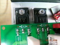
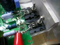
cuibono said:What are the clips on the chips for?
An audio expert shared a secret with me that these clips make sound much better! ..... Just kidding, I use them temporary to hold the heat sink.
I just finished a board with 49830 and IRFP240/9240x2. There is not oscillation.
I initially used "incorrect" resistor values for VBE multiplier which can give bias voltage over 20 V! During bias adjustment, I burned the chip and all four MOSFETs.
If driver stage MJE15030/15031 is added, the amp oscillates at 20 MHz. It can be stopped by increasing MOSFET gate resistors from 22 to 100 Ohm.
Attachments
Hi, Panson
In post 10 the thd level for lme49810 starts to rise at 2.5v with 1kohm.
This is because the output transistors in the chip are poor biasing,
substitute the r1 and r2 for a lower value (5 ohm for example) .
(please can you measure the current in R1).
in the Typical Application for lme49810 in first page of datasheet they use Rsb 2,2kohm withs is a very hight value.
The output transistor of the chip will switch for classb at 2.5ma (very bad) , i think a better value will be 680ohms.
This typical application, i think, was design (adapt) for a fender guitar power amplifier, and as you may know guitar amplifiers dont need to be very linear.
Tchau.
smms73 said:
In post 10 the thd level for lme49810 starts to rise at 2.5v with 1kohm.
This is because the output transistors in the chip are poor biasing,
substitute the r1 and r2 for a lower value (5 ohm for example) .
(please can you measure the current in R1).
Tchau.
Hi Tchau,
Thank you for your input. The Test circuit in data sheet uses 10 R as well. But it was not tested for 1kohm load. The problem was solved by using better heat sink. Please see this post http://www.diyaudio.com/forums/showthread.php?postid=1821187#post1821187
AndrewT said:Hi Panson,
when using 811 in the driver PCB what value for C8, or should it be left empty?
C8 is the cap across the output bias voltage.
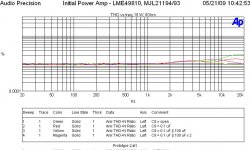
Hi Andrew,
I have data for 49810+21194/93 at the moment. Please see the curves below. The impact of C8 is noticeable in high frequencies. C8 = 0.1 uF || 100 uF gives the best result.
I will post 49811 result when it is ready.
Attachments
Here is 49811 preliminary result (THD vs freq, 18W, 8 Ohm). Output stage is triple-EF (pre-driver, driver and output device). The chip can not provide sufficient driving current for only one driver stage (MJE15030/31).
Without C8, there is a tendency of oscillation after excitation.
Without C8, there is a tendency of oscillation after excitation.
Attachments
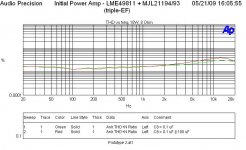
panson_hk said:After bias adjustment, THD vs freq of LME49811 is shown below. The output power is 18 W at 8 Ohm.
Very nice! What criterion did you use to set the bias?
Shaun said:
Very nice! What criterion did you use to set the bias?
The bias is adjusted to eliminate cross-over distortion which can be seen from THD residual.
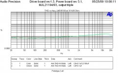
panson_hk said:I should use output triple instead of triple-EF to describe the output stage configuration (pre-driver, driver, output device).
Is that like a CFP driver? Could you please post this configuration? I would like to build a 300W amplifier...
Shaun said:
Is that like a CFP driver? Could you please post this configuration? I would like to build a 300W amplifier...
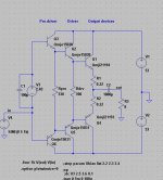
Hi Shaun,
This is a three stages of emitter follower as the SPICE model below.
Are you going to use CFP or EF output configuration?
Attachments
I have slightly modified the driver board. New boards are back from the fab house. Input, NFB ground and supply, decoupling ground are split as circled in the image. I have not found that this is essential for all 49810 built and tested so far. However, it seems necessary for 49811. 49811 seems to be a very sensitive chip. I am going to do more experiments.
Attachments
Shaun said:Which bipolar output board is intended for use with 49811?
ThermalTrak board and 3-lead board for MJL21193/94.
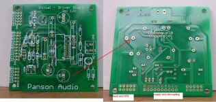
panson_hk said:Input, NFB ground and supply, decoupling ground are split as circled in the image.
C7, the decoupling cap, is tied into the Signal Ground trace.
The old PCB had C7 on a separate trace down to the multi-pin connectors.
You still have C2,3,4 & 8 as BIG caps with a long pin pitch.
Add an extra pin hole to R6 to allow three inline pot to be inserted.
AndrewT said:
C7, the decoupling cap, is tied into the Signal Ground trace.
The old PCB had C7 on a separate trace down to the multi-pin connectors.
You still have C2,3,4 & 8 as BIG caps with a long pin pitch.
Add an extra pin hole to R6 to allow three inline pot to be inserted.
Thank you Andrew!
Decoupling cap C7 & C3 is connected to the "dirty" ground as shown. This is identical to the previous PCB. C19, NFB cap together with input ground is connected to the "clean" ground of the board.
I will definitely do multi-hole for different cap sizes in new layouts.
Attachments
LME49830 on higher rails than output devices?
There's some great info here on the LME498xx parts but I can't find anyone who's running the chip on slightly higher rails than the output devices to improve the overall efficiency when using MOSFETs.
As many here probably know, on the same rails, MOSFETs tend to have around 10% - 20% less output power than bipolars. So while having 2 sets of rails adds complexity, it also increases power output and/or allows the amp to run cooler.
But will the internal output and bias scheme of the LME49830 work if its on higher rails than the output devices? And will the amp remain stable and happy when clipped (i.e. with the gate drive potentially swinging higher than the output voltage)? I'd rather not risk killing the chip and/or MOSFETs finding out if someone here knows one way or the other.
This might be best answered by SpittinLLama if nobody else here has experience with it? If there's already a post covering this, please just point me there?
- Status
- This old topic is closed. If you want to reopen this topic, contact a moderator using the "Report Post" button.
- Home
- Amplifiers
- Chip Amps
- Comparing LME49810, 49830 and 49811