I've found this in one of my service manuals. Hope it helps.
http://www.diyaudio.com/forums/attachment.php?attachmentid=259049&stc=1&d=1325995573
http://www.diyaudio.com/forums/attachment.php?attachmentid=259049&stc=1&d=1325995573
Attachments
One little problem I see in using the 2SK170 is it's maximum operating voltage of 40V. Using your DC measurement results in post #8 and by calculation shows ~43V across the JFET drain to source which is more than the maximum specified for the 2SK170. If you prefer on using the 2SK170, the cascode circuit needs to be tweaked to reduce the voltage going across the JFET.

The 2SK170GR is only a dollar each and available at mouser but one must buy enough to match pairs. Thanks
Last edited:
One little problem I see in using the 2SK170 is it's maximum operating voltage of 40V. Using your DC measurement results in post #8 and by calculation shows ~43V across the JFET drain to source which is more than the maximum specified for the 2SK170. If you prefer on using the 2SK170, the cascode circuit needs to be tweaked to reduce the voltage going across the JFET.
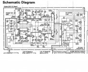
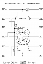
Wrong! The voltage across those cascoded FETs in DML-02 is clamped at 13.2V by 2SC1435 bipolars, so there's no problem in using 2SK170.
Captn Dave, what are you trying to achieve? Trying to recreate original DML-02 1:1 or trying to repair your preamp?
IMHO, using higher gm 2SK170 in place of 2SK129 or 2SK68, especially in phono stage would be an advantage - i.e. lower noise, but that would mean a slight redesign of DML-02 circuitry. By the way, Luxman moved to 2SK146/147 and even 2SK240 in their later designs - take a look at L-525 and L-530 phono stage schematics, for example.
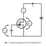
The voltage across the JFETs shouldn't be a problem. From the measurements in post 8:
Pin 4 is at +13.7 volts so the emitters of the cascode transistors (and the JFET drains) will be at about +13V.
The JFET sources are connected to pin 2, which is at +0.5 volts, so there's only about 12.5V across the JFETs.
[edit: oops, cross-post with elektroj]
Pin 4 is at +13.7 volts so the emitters of the cascode transistors (and the JFET drains) will be at about +13V.
The JFET sources are connected to pin 2, which is at +0.5 volts, so there's only about 12.5V across the JFETs.
[edit: oops, cross-post with elektroj]
take a look at L-525 and L-530 phono stage schematics, for example.
Point taken. The L-525 uses the same circuit. Thanks for the suggestion.
Lest there be any doubt, I wish to do this with current production parts if possible.
Attachments
Last edited:

Yay! I missed the voltage on pin 2 ")
The voltage across the JFETs shouldn't be a problem. From the measurements in post 8:
Pin 4 is at +13.7 volts so the emitters of the cascode transistors (and the JFET drains) will be at about +13V.
The JFET sources are connected to pin 2, which is at +0.5 volts, so there's only about 12.5V across the JFETs.
[edit: oops, cross-post with elektroj]
Last edited:
I have the devices bread boarded now and I have not yet got the circuit to work yet and could use a little advice.
I have used SK179 for the JFETS and BC560C and BC550C for the PNP and NPN, respectively, as gk7 was so kind as to suggest. I'm a little puzzled about the JFETs after it was suggested that the source should be at pin 2. The source of a FET is usually at a higher voltage than the drain correct? The 22K resistor is connected to the negative rail and the 220Rs are at the positive rail. So shouldn't the Drain be at pin 2? Please help me get that sorted out.
Next, as I understand JFETS, the gate needs to operate with a few volts of negative bias. At zero bias, the Device is open and at as the bias increase about about -4 volts the device should cut off. That's puzzling to me as well, because I measured about 16 volts at the center of the voltage divider (pin 4). One would expect the emitters of the NPNs to be close to that voltage too, right? So that voltage puts Vsg well above cutoff if I'm thinking correctly.
So that's where I am, measuring about 15 volts on the emitter and so the FET is at cutoff and I'm passing no signal.
Lets stop for now with those two questions. Once I get that sorted the other questions will probably be moot.
Thanks
Attachments
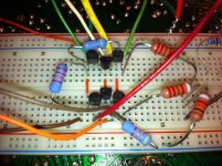
I have the devices bread boarded now and I have not yet got the circuit to work yet and could use a little advice.
Captn Dave, I hope you're not testing your differential stage 'stand alone' i.e. without the rest of the Luxman circuitry.
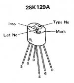
You mean 2SK 170. not 179, right? What selection grade, by the way - GR or BL? Did you matched them?I have used SK179 for the JFETS
That is correct... it was suggested that the source should be at pin 2.
No, the other way around. See attachment.The source of a FET is usually at a higher voltage than the drain correct?
Relative to the source, one should add. If your gates are at 0V, sources should be at some positive potential. In case of 2SK170s not more than +0.2.. +0.5 Volts.Next, as I understand JFETS, the gate needs to operate with a few volts of negative bias.
Sounds ok.I measured about 16 volts at the center of the voltage divider (pin 4).
Yes, the same voltage minus 0.7 volts (one Vbe drop)One would expect the emitters of the NPNs to be close to that voltage too, right?
No, you're notSo that voltage puts Vsg well above cutoff if I'm thinking correctly.
Please measure all voltages on all pins of your selfmade DML-02 and post them.
P.S. With so much wiring it is possible that your circuit is oscillating.
---
Attachments
Last edited:
I have the devices bread boarded now and I have not yet got the circuit to work yet and could use a little advice.
I have used SK179 for the JFETS and BC560C and BC550C for the PNP and NPN, respectively, as gk7 was so kind as to suggest. I'm a little puzzled about the JFETs after it was suggested that the source should be at pin 2. The source of a FET is usually at a higher voltage than the drain correct? The 22K resistor is connected to the negative rail and the 220Rs are at the positive rail. So shouldn't the Drain be at pin 2? Please help me get that sorted out.
Next, as I understand JFETS, the gate needs to operate with a few volts of negative bias. At zero bias, the Device is open and at as the bias increase about about -4 volts the device should cut off. That's puzzling to me as well, because I measured about 16 volts at the center of the voltage divider (pin 4). One would expect the emitters of the NPNs to be close to that voltage too, right? So that voltage puts Vsg well above cutoff if I'm thinking correctly.
So that's where I am, measuring about 15 volts on the emitter and so the FET is at cutoff and I'm passing no signal.
Lets stop for now with those two questions. Once I get that sorted the other questions will probably be moot.
Thanks
Hi Dave,
As I have following amplifiers standing behind me :
L58a, L100, M12, B12, L11, C12, C02, C03 all working.
I would like to hear whether you have solved the DML02 secret, because research has told me that the original Luxman fet's used is unobtainable.
Rgds Gudmund
No I did not.
I built up a circuit using the devices suggested and it did not work as I expected it to. There is a very real possibility that there are other issues at play in the circuitry outside the DML02 that may be effecting my results. The circuit boards on the C12 are very poor quality and it has become very difficult to continue with this project given the lifted and broken traces. I have set it aside in favor of more interesting projects for now.
I wish I had better news.
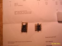
EDIT: My poor results may also be a result of my poor understanding of the circuits involved. I would encourage you to give it a try. Do any of the amps you have there contain a Luxman workaround DML02 card like the one depicted in the photo posted in this thread? That would be a very good place to start.
Dave
I built up a circuit using the devices suggested and it did not work as I expected it to. There is a very real possibility that there are other issues at play in the circuitry outside the DML02 that may be effecting my results. The circuit boards on the C12 are very poor quality and it has become very difficult to continue with this project given the lifted and broken traces. I have set it aside in favor of more interesting projects for now.
I wish I had better news.
EDIT: My poor results may also be a result of my poor understanding of the circuits involved. I would encourage you to give it a try. Do any of the amps you have there contain a Luxman workaround DML02 card like the one depicted in the photo posted in this thread? That would be a very good place to start.
Dave
Last edited:
Captn Dave, I hope you're not testing your differential stage 'stand alone' i.e. without the rest of the Luxman circuitry.
You mean 2SK 170. not 179, right? What selection grade, by the way - GR or BL? Did you matched them?
That is correct.
No, the other way around. See attachment.
Relative to the source, one should add. If your gates are at 0V, sources should be at some positive potential. In case of 2SK170s not more than +0.2.. +0.5 Volts.
Sounds ok.
Yes, the same voltage minus 0.7 volts (one Vbe drop)
No, you're not
Please measure all voltages on all pins of your selfmade DML-02 and post them.
P.S. With so much wiring it is possible that your circuit is oscillating.
---
I'm testing it within the larger circuit.
That 179 was a typo. I used the SK170GRF.
I'm testing it within the larger circuit.
That 179 was a typo. I used the SK170GRF.
Found as follows:
DML-02 components : 2SK240 ( 2 x 2SK170 matched) , 2 x 2SA836 , 2 x 2SC1345
DML-01 components : IC NEC uPA 63A , 2SC1775 x 2 , 100R x 2
Found the NEC uPA63 by "Little Diode" to 7,99£ and the NEC uPA63H to 3,99£ , at last the NEC uPA 63HI to 7,99£ ...can't find the difference???
May be the NEC datasheet uPA1556 match the uPA 63A?
Compared to the drawn schematics of the DML-01 and the DML-02 at:
https://picasaweb.google.com/103176186685392443797/LuxmanC12Preamplifier#5636906491154070882
The mentioned components seems to match.
Luxman C12 & M12 repair
Luxman C12 & M12 repair:
https://picasaweb.google.com/103176186685392443797/LuxmanC12Restoration
https://picasaweb.google.com/103176186685392443797/LuxmanM12Restoration
Luxman DML-01 & DML-02 :
https://picasaweb.google.com/103176186685392443797/LuxmanC12Preamplifier
Found as follows:
DML-02 components : 2SK240 ( 2 x 2SK170 matched) , 2 x 2SA836 , 2 x 2SC1345
DML-01 components : IC NEC uPA 63A , 2SC1775 x 2 , 100R x 2
Luxman C12 & M12 repair:
https://picasaweb.google.com/103176186685392443797/LuxmanC12Restoration
https://picasaweb.google.com/103176186685392443797/LuxmanM12Restoration
Luxman DML-01 & DML-02 :
https://picasaweb.google.com/103176186685392443797/LuxmanC12Preamplifier
Has anybody come up with a final determination of the schematic and actual currently available parts, with hopefully a working example of these cloned Luxman DML 02's? I am in need of about 6.
I have the 10. of july 2012 bought one pcs. of DML-01 and one pcs. of DML-02 modules ("IC") from :
"HiFi-service vom Feinsten" ....Luxman -forever
Contact: dieter.kuehnhold@yahoo.de
The price of DML-01 : 24,90€ = 30,60$
The price of DML-02 : 31,50€ = 38,70$
Plus shipment
Mr. Kühnhold has made new PCB's and uses K240BL , C1345 and A836 for the DML-02.
NEC uPA63H and C1775 for the DML-01. see attached file, or:
https://picasaweb.google.com/103176186685392443797/LuxmanC12Preamplifier#5766972386284195138
It's rather expensive if you need six modules! ...might try to make the PCB's, but what about the component's?
rgds.
Attachments
Last edited:
- Status
- This old topic is closed. If you want to reopen this topic, contact a moderator using the "Report Post" button.
- Home
- Amplifiers
- Solid State
- Cloning the Luxman IC known as DML-02