Thanks for the reminder.
In this design the Star grounding point is supposed to locate on a separate PSU board, not on this PCB. Grounding will be done by chassis wiring. The amplifier PCB has a ground system consists of a few separate ground nets that are to be wired to the start point on the PSU individually. The grounding connectors are J14 for the IPS "clean" ground, J7 for the small signal power supply return, and J8/J18 for the o/p stage rail decoupling return. So they never mix up on the amp PCB.
The speaker return will go directly to the star ground.
There is a possibility, however, up to the chassis layout design and location of the reservoir caps, that J18 be made the star point. And that is the reason why J18 is a big heavy 6-pin PowerTap connector.
I don't get "Also, sometimes it is good to add decoupling between power amp output and driver/ltp stages." could you be a bit more specific? Thanks.
Last edited:
Thanks for the reminder.
I don't get "Also, sometimes it is good to add decoupling between power amp output and driver/ltp stages." could you be a bit more specific? Thanks.
I have found with some amp designs you need to put a resistor and capacitor in series from the b+ and b- rails to the driver stages to stop hum.
I have found with some amp designs you need to put a resistor and capacitor in series from the b+ and b- rails to the driver stages to stop hum.
Why would that work? I have not seen many amplifiers perhaps that's why it sounds much like a "bandage" solution to me. The IPS/VAS stages have a pair of separate faston connectors on my PCB. They either share power rails with o/p, by shorting J6 to J2 and J5 to J1, or instead take power from an off-board regulated supply at a few volts higher than that of o/p stage. Perhaps the R-C network you mentioned would be used in the latter case, but I'm not sure it is a good idea to inject noise on the o/p rails to the clean regulated front stage rails.
Why would that work? I have not seen many amplifiers perhaps that's why it sounds much like a "bandage" solution to me. The IPS/VAS stages have a pair of separate faston connectors on my PCB. They either share power rails with o/p, by shorting J6 to J2 and J5 to J1, or instead take power from an off-board regulated supply at a few volts higher than that of o/p stage. Perhaps the R-C network you mentioned would be used in the latter case, but I'm not sure it is a good idea to inject noise on the o/p rails to the clean regulated front stage rails.
If you are using a separate higher voltage rail then that is fine.
Where the amplifiers driver/LTP stage supply is also connected to the output transistor voltages you can get modulation of the supply passed back to the input.
I have found in practice you can get almost zero hum with no input signal if you add in the components I mentioned.
Hi,
Solid State relay... but why?
I doubt that this solution is better than a normal relay. Distortion?
You could use more than one feedback path/loop. One before relay and one after relay.
That could reduce any non linear behaviour of your solidstate relay.
Rotel has used this two feedback loops in some of their amps.
What is your openloop gain in this amp? (Estimated)
To be honest, your design looks a bit overkill to me, but I wish you good luck getting it build!
Cheers
Flemming
By nigelwright7557 -Where the amplifiers driver/LTP stage supply is also connected to the output transistor voltages you can get modulation of the supply passed back to the input.
This is where the global NFB /PSRR of a (standard) amp comes into play. The simple C/R/C
filter between OP and VAS/LTP will increase PSRR 6db across most of the audio band.
I have never experienced actual hum while running a single supply NFB amp ,although a separate supply for the LTP/VAS will make the amp more linear with far less distortion at high power levels.
This amp seems not to have the output stage included in the feedback loop except for DC , so a split supply is more crucial here. Still , after prototyping a similar amp (krill ... OP stage not included in the feedback loop) , hum was never a factor - just more distortion.
The DIY amp (badger) has C/R/C as a standard option but can be powered by a separate supply if chosen. I have not heard any difference between these options at normal
 listening levels.
 To be honest, your design looks a bit overkill to me, but I wish you good luck getting it build!
Not overkill ! Just a good design. I discussed the diamond buffer triple with Mr. Cordell in his book thread and even prototyped it (awesome sub amp -2R loads). My only concern with the above circuit is the anemic drivers (Q11/12 -MJE15032/33). Mine had NJW3281/0302 - small outputs ! as the drivers with 4 pair actual outputs. good luck !! - this is a good amp ... like a leach on steroids brought into the 21st century
.OS
@OS, thanks for bringing the insight of NFB/PSRR, and you experience speaks a lot.
I much appreciate your comment about the driver transistors. I used the MJE15032/33 in my modified Leach amp (google pimped citation) to drive 5 pairs of NJL3281/1302 ans have had no complains. I never used that amp on a 2-R load though, just my good old PSB Stratus Gold i speaker 4-R rated. In a diamond buffer tripple set up, the maximum available current into the base of a driver transistor is limited by the 10-mA CCS at pre-driver's load, would you think a bigger driver transistor can help? I never thought of using a small o/p transistor as a driver in an amp up to 300W, but I'll look into the layout and see if a TO3P can go in there.
The circuit I posted does have the o/p stage inside the f/b loop. Perhaps the way I drew the schematic was a bit misleading --- the old style schematic can only have a tie dot at a T junction.
@Flemming, "Solid State relay... but why" That's one less mechanical contact that can haunt you in the back of your mind: the spark/arc may have not done anything to it, it may still be as good as last week, and I'm still hearing the full potential of my amp...
..and most importantly, since this is a solid state forum, I guess anything solid state is encouraged or recommended?
R33 - 10ma??
R33 and the two drivers are at hundreds of mA's , not 10. The 2 CCS's regulate only the diamond predrivers in your circuit. I was just concerned with the SOA of the MJE's.
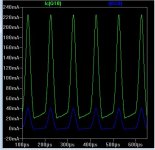
See below for the real deal (simulation of my triple).
Blue is just the current across one base stopper on an output and green is the total dissipation of the positive driver. This is with a 4R load.
Another consideration is the thermal coefficient of the diamond and drivers are linked in this amp (they cancel each other out) , leaving only the outputs Vbe remaining to compensate for. This would require a separate heatsink for the drivers and the diamond. Just a thought . In other words , this amp is not compensated for in the same manner as a typical triple (leach).
os
R33 and the two drivers are at hundreds of mA's , not 10. The 2 CCS's regulate only the diamond predrivers in your circuit. I was just concerned with the SOA of the MJE's.
See below for the real deal (simulation of my triple).
Blue is just the current across one base stopper on an output and green is the total dissipation of the positive driver. This is with a 4R load.
Another consideration is the thermal coefficient of the diamond and drivers are linked in this amp (they cancel each other out) , leaving only the outputs Vbe remaining to compensate for. This would require a separate heatsink for the drivers and the diamond. Just a thought
. In other words , this amp is not compensated for in the same manner as a typical triple (leach).os
Attachments
@OS, I like that wave form chart.
By 10 mA I was referring to the available current into the base of the driver transistors. Not the collector current your chart was showing. If I understood the diamond buffer triple correctly, the CCS at the emitter of the pre-drivers in fact limits the current into the base of the drivers.
If the driver transistors have an Hfe of 100 the maximum they can possibly put out to the output transistors would be about 1A. This probably can be viewed as a current limiting protection mechanism intrinsic to a diamond buffer triple -- you can't go too far into the north in the SOA chart.
I think you're right about using NJW0281/0302 as drivers. They are several times more robust than the MJEs in SOA, and stand a much better chance when a fault condition occurs. I was able to move things around and the PCB now can have TO-3P drivers.
I prototyped the DBT myself a while back, with a scaled down circuit having only one pair of NJL3281/1302 at o/p and a +55V rail. The op-amp based bias control worked very well. I found the thermally-coupled MJE drivers and the TO-126 pre-drivers don't cancel their tempco completely. There was a little bit of residue tempco between them, but, since the heat sink they share doesn.t have much temperature swing, I don't see a trouble there.
On my PCB design the pre-drivers and drivers in the DBT are again on their own heat sink, they are mounted on opposite sides of an aluminum plate and share a same bolt. The size of the heat sink, however, may have to be larger than the size the PCB silkscreen indicates. As it has to dissipate 7-8W heat.
Attachments
I'm glad you like it, Piersma.Thank you for the kind words.
"Connect cathode of D10 to the emitter of Q15." --- why does it sound like put a tiny bit of bleach in the coffee and you'll get a new dimension of flavor? Sorry, no offense here, I'm relatively new and halfhearted to audio, and that kind of circuit looks way over me. Kindly details please. Thanks again.
"Connect cathode of D10 to the emitter of Q15." --- why does it sound like put a tiny bit of bleach in the coffee and you'll get a new dimension of flavor? Sorry, no offense here, I'm relatively new and halfhearted to audio, and that kind of circuit looks way over me. Kindly details please. Thanks again.
Seems like you wanna push the distortion boundries with this amplifier.
Connect cathode of D10 to the emitter of Q15.
I like you amp, good luck simulating and building. (like OS always does!)
regards,
Piersma
Maybe not the distortion boundaries , but the sound will be supurb .
Having the output stage out of the AC feedback loop has it's advantages.
One being that the "re- activeness" of the loudspeaker load will not be
reintegrated into the NFB signal. I've seen NIKKO amps and others that use this technique and they sound superb. The LTP/VAS will have PPM distortion with the DB output stage at around <.01% or less .... realistically.
Can't wait to see it .. Nattawa !
OS
- Status
- This old topic is closed. If you want to reopen this topic, contact a moderator using the "Report Post" button.
- Home
- Amplifiers
- Solid State
- Circuit and PCB layout review will be appreciated