A couple more ideas that came from some experiments:
1) You can think of a CFP as a complex transistor. To the stages in front, it looks like the 'driver' itself. This means that you can parallel two complete CFPs. In this manner you can save one emitter resistor drop. The downside is, the B-E resistor of the power BJT must be well chosen in order to get approximately same currents through the driver and power BJTs at low currents. There is another way around this, see below.
2) Use (schottky) diodes in parallel with emitter resistors. Since normal quiescent current setting make only millivolts of voltage across Re, the diodes will only do their job at higher currents. At the same time, their Rd depends on the current and you get a sort of variable Re. This can only work properly as long as the diodes do not conduct small fractions (perhaps 1%) of quiescent current in quiescent conditions. Higher than that will produce thermal instability. It does have other uses as well which are outside the scope of this thread.
3) Most fast high power BJTs are made out of arrays of smaller cells with ballast resistors - in actuality, small transistors with integrated emitter resistor, connected in parallel. The usual name for this construction is LAPT but some manufacturers use other names. This means the transistor itself actually has a form of integrated emitter resistance. It also usually has a slight positive temperature coefficient. The value is normally around 0.05-0.15 ohms, depending on transistor size and actual technology specifics. If a Ic vc Vce graph is given, such transistors can be recognized by the almost sompletely linear slope offset by the Vbe treshold, which means the emitter resistor linearizes the usual exponential slope. The equivalent Re can be calculated from the angle of the slope. Sanyo 2SB817/2SD1047 are an excellent example. These transistors can be used without emitter resistors as a single pair, with proper thermal tracking of the bias servo transistor. These kinds of power BJTs work very well in a CFP becasue the built-in Re results in a better defined gain, so chosing the right Rbe for the power BJT in a CFP is easyer and less critical when you need to make matching CFP combos.
4) one thing which can often be noticed with transistors as described above, is that the equivalent Re often differs between the PNP and NPN part, from the slopes in the datasheet, about 0.13 ohms for the 2SB817, and .1 ohms for the 2SD1047. Best results with such transistor pairs are obtained when different external Re is sued for the PNP and NPN part, compensating this difference. In fact, it is possible to use just the extra .033 ohms on the NPN part. In a similar manner, it is possible to 'pair' transistors that usually do not make proper complementary pairs, by using different external Re. Note Vce for Vbe vs Ic measurement - on the 2SB817/2SD1047 datasheet - only 5V. It is possible to measure equivalent internal Re in 'home conditions' with this low Vce up to about half the maximum Ic and proper transistor cooling, as it will prevent secondary breakdown for 99.9% of all power BJTs, so pairs can be selected (with or without external Re tweaking).
Interesting. But I do not get wich Re you are about. Could you please scketch a schematic?2) Use (schottky) diodes in parallel with emitter resistors. Since normal quiescent current setting make only millivolts of voltage across Re, the diodes will only do their job at higher currents. At the same time, their Rd depends on the current and you get a sort of variable Re. This can only work properly as long as the diodes do not conduct small fractions (perhaps 1%) of quiescent current in quiescent conditions. Higher than that will produce thermal instability. It does have other uses as well which are outside the scope of this thread.
some of the above things need to be tested in real life.....
real life tests on stress stability and so on and on will proove right ...simulations only is not enough ...add also that CFP are more pcb sensitive than classic EFP and things get tricky
greek guy tryied an sziklai builted on this concept ( each output had its dedicted driver ) but was a nightmare to stabilize .... even with large Miller caps on the drivers offset was a mess , bias was a mess , and performance badwidthwise was also terrible ..
dont want to be a killjoy but still we also have to keep in mind that amps in some time of their life will be stressed ...
Interesting. But I do not get wich Re you are about. Could you please scketch a schematic?
This would be the Re for the 'compound BJT' that the CFP combo actually makes, so the one from (driver E + power C) going to the amp output.
Using this approach is only valid for single pairs, if more power BJTs are to be paralleled, this needs to be done the traditional way. The reason is that adding a schottky to each Re in parallel BJTs will result in very bad current sharing at high currents, where proper current sharing is most important. Transistors with built-in Re of some sort may be an exception, if they are taken from the same gain group, as internal Re may insure good enough current share - but this is something that needs to be investigated.
some of the above things need to be tested in real life....
greek guy tryied an sziklai builted on this concept ( each output had its dedicted driver ) but was a nightmare to stabilize .... even with large Miller caps on the drivers offset was a mess , bias was a mess , and performance badwidthwise was also terrible ..
I was talking about a real world experiment, not simulation, but I do agree.
CFP in general has the 'fast driver, slow output, NFB into fast driver' problem, which is an open invitation to oscillations. There are opposing requirements re current drive of the power BJT and potential oscillations. Generalizing about a real-world CFP implementation is almost impossible - unlike EF variants, the choice of BJTs for a CFP is crucial, and dictates stability measures if needed.
What I proposed was done on a small scale (fast outputs) and it works well - but I can certainly immagine that something like classic BD139/140 driving TO3 4MHz BJTs will be a big problem. CFP needs to be stabilized within itself, not by adding overcompensation to the amplifier. Also, it has a propensity to reflect negative input impedances at HF - base stoppers for drivers and outputs are often a must, along with other measures (sometimes even deliberately adding Re to the power BJT in order to get more desirable current ratios for criver and power BJT), not to mention attention to stray capacitances and adding extra capacitors in various places.
Surprisingly, I have done a diamond-buffer CFP output follower using BD139/140 and 2SC5200/2SA1943 and it required only a base stopper at the very input to stabilize with low impedance sources. This was done on perfboard, but it's a very tight construction with local decoupling, and it even has bootstrap 'current sources' and a form of error correction built in. I expected huge problems with it but it turned out tame. On the other hand, I've done an old style quasicomp with MJE15030 and 2N3773 as the PNP side and it was a nightmare to get working

Last edited:
Could you enlight us with some schematic?Surprisingly, I have done a diamond-buffer CFP output follower using BD139/140 and 2SC5200/2SA1943 and it required only a base stopper at the very input to stabilize with low impedance sources. This was done on perfboard, but it's a very tight construction with local decoupling, and it even has bootstrap 'current sources' and a form of error correction built in. I expected huge problems with it but it turned out tame.
effebi
Could you enlight us with some schematic?
effebi
I did this for someone else so the IP is not mine any more.
Basically, use a diamond buffer as a start, add emitter resistors into the output complementary of it, and a small offset voltage between the input complementary transistors bases, then convert the output pair to a CFP, and reduce emitter resitors by an appropriate factor so it's a power follower. This is the basis of the topology. Some juggling of the connection between the CFP output collectors and previous stage (the output of the diamond buffer) emitters implements a different type of local feedback which may be viewed as an error correction scheme.
Thanks a lot for your efforts. While I fully understand your IP issues ( I have same problems with my job) , then you must realize why in engineering a drawing is worth more than 1000 words.
If you add up the language barrier, that's it. You might well have written it in Slavic Language (that I'll love to learn sooner or later) the result would be the same for me. Pity.
Something like this...
Attachments
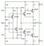
Something like this...
Well, nice, thank you.
I believe (not sure, really) I have seen somethig like that in some textbook many years ago (is it an RCA circuit?).
But as long the CFP is concerned, it looks to me pretty much standard, except only maybe the OP base stoppers. I did not know that the two transistors in input constitute a diamond-buffer. I just guess that the two huge capacitors are bootstrapping them. I will have to look back to that neat solution.
More than all, this thread was about MULTIPLE PAIR CFP solutions, and I haven't seen many yet. Anyone .....?
Something like this...
Have you tried to connect bootstraped caps to CFP divers BCxyz instead of output?
Won't be the Schottky internal resistance enough to allow some sharing, if the OPs of each rail are reasonably well matched? Maybe is up to device(diode) choice.This would be the Re for the 'compound BJT' that the CFP combo actually makes, so the one from (driver E + power C) going to the amp output.
Using this approach is only valid for single pairs, if more power BJTs are to be paralleled, this needs to be done the traditional way. The reason is that adding a schottky to each Re in parallel BJTs will result in very bad current sharing at high currents, where proper current sharing is most important. Transistors with built-in Re of some sort may be an exception, if they are taken from the same gain group, as internal Re may insure good enough current share - but this is something that needs to be investigated.
Have you tried to connect bootstraped caps to CFP divers BCxyz instead of output?
Yes but in this case the emitters of CFP drivers (second stage of diamond buffer) and collectors of the power BJTs are not exactly connected like in the picture, there is a network of passive components constituting an EC scheme in the real version, so the bootstrapping cannot be taken from there. There is a whole lot of finesse missing from that circuit, it's only shown in principle even though it will work as drawn.
Won't be the Schottky internal resistance enough to allow some sharing, if the OPs of each rail are reasonably well matched? Maybe is up to device(diode) choice.
Depends on the diode, but as all diodes, Schottky's internal resistances drop with current increase - and they have to be dimensioned to carry the full current of that power BJT, so quite large - therefore Rd is quite small. The internal resistance of a array-constructed BJT (like LAPT) will be more than that, so if you reasonably match them, it should still work well.
Hi,
the circuit with bipolar transistors exhibits poor DC symmetry, R7-8-10-11-12-13 aggravate the switching performance problem, most importantly, T4-5 should better be a FET. The role of T3-6 is kinda crucial and complex, they deserve to be chosen with care.
the circuit with bipolar transistors exhibits poor DC symmetry, R7-8-10-11-12-13 aggravate the switching performance problem, most importantly, T4-5 should better be a FET. The role of T3-6 is kinda crucial and complex, they deserve to be chosen with care.
Attachments
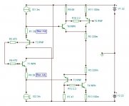
Hi,
the circuit with bipolar transistors exhibits poor DC symmetry, R7-8-10-11-12-13 aggravate the switching performance problem, most importantly, T4-5 should better be a FET. The role of T3-6 is kinda crucial and complex, they deserve to be chosen with care.
Agreed, also they must be well thermally coupled. As i said, the schematic is only given in principle, it's not by any means optimized (for instance, parts are given as available in my simulator in order to draw the schematic, not provide maximum performance). In your schematic DC conditions are for all intents and purposes undefined as it relies solely on beta and leakage for input biasing. Note that the 0.1 ohm resistors in my original schematic mimic the built-in emitter resistance of the transistors I actually used and also to be able to monitor Ie in certain conditions. In most traditional CFP schematics they will be 0 ohms.
However, I have reservations about making the power transistors (MOS)FETs. BJT-MOSFET CFP has the obvious advantage (if well dimensioned) that, unlike a typical BJT CFP, you don't get a fast device driving a slow one which is then tied into a feedback loop - the delay of the slow device is an invitation to oscillation. MOSFETs can be quite fast. However, there is one not so obvious disadvantage, and that's what happens if the output goes into current clipping/limit, say on a low impedance/heavily reactive load. The BJT part will happily drive the gates of the MOSFETs right down to the potential of the drain, which may be more than Vgsmax. There is really no simple way to solve this problem without degrading the performance of the circuit, in a similar way that chosing a set of R7-13 is always a compromise. In the classic CFP, the power device usually also has q rather high base current maximum, easily far over the maximum collector current of the BJT 'driver', so the whole thing really looks like a high-gain BJT without adding extra problems that may not be visible outside (oscillation notwithstanding, but then a BJT-MOSFET one is not trivial in this matter as well).
Last edited:
- Status
- This old topic is closed. If you want to reopen this topic, contact a moderator using the "Report Post" button.
- Home
- Amplifiers
- Solid State
- CFP multiple output pairs.