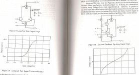
Meanwhile, MB - I think you will find your answere(s) in this book ->
It also explains why for competitive reasons the processes, and actual model the mfr uses are hidden or disguised in an opa form with simplified engineering formulas. The real design is not disclosed nor the real models used. So, you have incomplete info and data to use.
A more accurate model is shown for you to use that models CFA better than what mfr supply. AFTER, you have read this booklet, then see if you have any questions left. It is the best summery of the art as it was emerging 10 years ago and covers all the basic derivitives.
You ought to find it very helpful.
Thx-RNMarsh
It also explains why for competitive reasons the processes, and actual model the mfr uses are hidden or disguised in an opa form with simplified engineering formulas. The real design is not disclosed nor the real models used. So, you have incomplete info and data to use.
A more accurate model is shown for you to use that models CFA better than what mfr supply. AFTER, you have read this booklet, then see if you have any questions left. It is the best summery of the art as it was emerging 10 years ago and covers all the basic derivitives.
You ought to find it very helpful.

Thx-RNMarsh
Last edited:
For audio apps, I think this next point is important to obtaining low distortion over a wide band of freqs --->
"Fundamentally, voltage and current are associated to electric charge. Driving charge into high impedance nodes will result in large voltage excursion, whilst charge driven into low impedance nodes will result in small voltage excursions".
So? Disregarding the speed implications which have been the feature exploited the most for RF needs ---
Well, this (small voltage swing) is important for low distortion with devices and their non-linear capacitances and characteristics. It can also lead to simpler (better?) circuits. So we start off with a Plus situation for audio before we even consider NFB in the picture. If this important feature is not compromised, but recognised and kept intact, then the design will have the best chance of meeting audio goals.
Thx-RNMarsh
Last edited:
I don't know this book Richard but if it is as good as it's predecessor I have, it's well worth to get it.
"Analogue IC design: the current-mode approach", from 1990 published by Peter Peregrinus for the IEE, 3rd author replaced by D. G. Haig.
jan
Its the summery of the technolgy... more complete over all view.
-RM
For audio apps, I think this next point is important to obtaining low distortion over a wide band of freqs --->
"Fundamentally, voltage and current are associated to electric charge. Driving charge into high impedance nodes will result in large voltage excursion, whilst charge driven into low impedance nodes will result in small voltage excursions".
So? Disregarding the speed implications which have been the feature exploited the most for RF needs ---
Well, this (small voltage swing) is important for low distortion with devices and their non-linear capacitances and characteristics. It can also lead to simpler (better?) circuits. So we start off with a Plus situation for audio before we even consider NFB in the picture. If this important feature is not compromised, but recognised and kept intact, then the design will have the best chance of meeting audio goals.
Thx-RNMarsh
So well said. I am kinda excited about this thread, even if most will be over my head. Thanks to all who started it.
Its the summery of the technolgy... more complete over all view.
-RM
You need to be careful here a larger picture could contain more of what IC folks consider current domain, multipliers, log amps, RMS converters, log domain filters, etc. In general CFA type amplifiers are a small side show.
To the Current-Mode approach --
Laying down more requirements to be a current-mode amp -->
"The circuit demands symmetrical processes with fully complementary transistors (mostly BJT in our use) that closely match. In the developed processes to make CMA, dielectrically isolated transistors are able to create seperate transistors and are vertical and their performance characteristics are much more closely matched."
Matched complementary stages... .
Thx-RNMarsh


Laying down more requirements to be a current-mode amp -->
Matched complementary stages... .
Thx-RNMarsh
View attachment 365682
Is that how that other stuff translates? It was meaningless to my compromised mind.
Just a few more coming --- got to get some other things done -- like eat something! be back soon --
dont go anywhere - i'll try to pull it together for you, later.
meanwhile get a group-buy or someway to get that book on the subject, models etc. see line #55, above.
'cause I aint going to write it all here for ya.
-RNM
dont go anywhere - i'll try to pull it together for you, later.
meanwhile get a group-buy or someway to get that book on the subject, models etc. see line #55, above.
'cause I aint going to write it all here for ya.
-RNM
Last edited:
Richard,
Will try and add a bit to your curves above.
(I've posted this before mostly because I found it interesting, I dont think anyone else does):
For the cfa there is (approximately) a fixed voltage across the two bases. Ignoring the error current flowing into the feedback network, as the input changes the feedback node (the negative input, where the degeneration resistors are common) will also change. Since there is a constant voltage across the bases the amount of b-e change (in opposite directions) is the same for each transistor. It is the non-linear difference between these b-e voltages than constitutes distortion.
Now if you think of these voltages superimposed on the exponential i-v curve of each transistor you will see, equal and opposite voltage movements from the bias point, the resulting changes in collector currents for each are significantly different (and non-linear). It is this current difference which flows through the high impedance gain node, supplies feedback and determination of the error or delta Vb-e (approximately equal but opposite directions for each transistor).
In contrast for an ltp, there is no voltage constraint across the bases, but rather a constraint that the sum of collector (emitter) currents remain constant.
Conversely as the input voltage changes the collector currents will change (equal and opposite amounts). If this is viewed from the same inherent exponential i-v curve there is a symmetrical linear delta on the current axis (analogous to the cfa voltage axis) resulting in two non-linear and different base emitter voltages. The difference in these two base emitter voltages is basically the distortion at the feedback point.
The net is an ltp will show much more linear collector currents as a function of vin, with the corresponding exponential appearing as distortion across the base emitters, whereas the cfa will show very linear base emitter changes as a function of vin with the corresponding exponential appearing on the collector currents.
Thanks
-Antonio
Laying down more requirements to be a current-mode amp -->
"The circuit demands symmetrical processes with fully complementary transistors (mostly BJT in our use) that closely match. In the developed processes to make CMA, dielectrically isolated transistors are able to create seperate transistors and are vertical and their performance characteristics are much more closely matched."
Matched complementary stages... .
Thx-RNMarsh
View attachment 365682
Hi Richard,
I think we need to be careful to distinguish current-mode analog signal processing from current feedback amplifiers. In a CFA the signal feedback can be considered a current, but that is all there need be in the current domain. Put another way, in a CFA the error amplifier reacts ideally to a difference (error) of currents, while in a VFA the error amplifier reacts to a difference (error) in voltages. The impedance that the feedback network sees at the error amplifier is largely what differentiates the two. The CFA feedback network sees a low impedance ideally, while the VFA feedback network sees a high impedance ideally.
It is important to realize that the voltage at the feedback node of a CFA is not necessarily zero; it is often equal to the input voltage to the amplifier, as in a non-inverting CFA. But you can also view the CFA feedback network as operating as a voltage divider that seeks to produce a voltage that is the same as the input voltage for a non-inverting CFA. If it does not produce the same open-circuit voltage, then an error current will flow. There can be many ways to look at this. Sort of like how given source and network has Thevenin and Norton equivalents. In fact, I seem to recall CFAs as being described as Norton amplifiers. I could be wrong about that, however.
I think that the classic RIAA preamp, wherein the RIAA feedback network connects to the emitter of the input transistor, is in fact a CFA.
I hope that my assertion that the CFA can be viewed in more than one way has not confused matters.
A better example of current-mode analog signal processing is the cascomp input stage, where the signal current from an input LTP is summed with an error correction current at the emitters of a cascode.
Cheers,
Bob
PS -- GET THE BOOK !!Magno, BobCo.... very nice replies for clarity. helps everyone as we distill this down to what it means to be a CMA. I dont want to be the point man on this... I just need to set a focus and direction to move the conversation and issues in a more clear and direct way.
It had come to remind me of trying to corral or hurd cats. Ever try that? Hurding cats. It isnt possible... they go all over the place in every direction... except for food and sex, you'll never get them to stay on the subject you are dealing with. But now, this is a lot better with a forum devoted to one topic. We sound like educated, respectful gentlemen again.
So, without further adooo -->
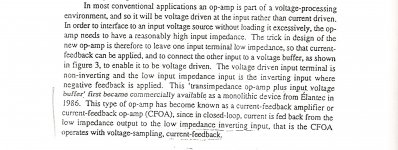
This and the elements posted earlier is what i developed years before the 'final' version via Elantec (with Current-Conveyer/Current-Mirror) came forth onto the world scene and changed the landcape. It was published in TAA.. now taken over by Elektor and probably never to be seen again. However, the recap/over-view and Time-Line is now in Linear Audio issue Vol 3. The original design topology was later made into an all FET circuit and popularized by E.Borbeley.
If your design fits all the above minimum, then its a CMA. Anything else and all bets are off.
back over to you guys --- take it away... but be good and help us all enjoy the journey and learn from one another...... [he said in a grand-fatherly way] Time for specifics and details? Now, what was the question?
THx-RNMarsh
It had come to remind me of trying to corral or hurd cats. Ever try that? Hurding cats. It isnt possible... they go all over the place in every direction... except for food and sex, you'll never get them to stay on the subject you are dealing with. But now, this is a lot better with a forum devoted to one topic. We sound like educated, respectful gentlemen again.
So, without further adooo -->

This and the elements posted earlier is what i developed years before the 'final' version via Elantec (with Current-Conveyer/Current-Mirror) came forth onto the world scene and changed the landcape. It was published in TAA.. now taken over by Elektor and probably never to be seen again. However, the recap/over-view and Time-Line is now in Linear Audio issue Vol 3. The original design topology was later made into an all FET circuit and popularized by E.Borbeley.
If your design fits all the above minimum, then its a CMA. Anything else and all bets are off.
back over to you guys --- take it away... but be good and help us all enjoy the journey and learn from one another...... [he said in a grand-fatherly way] Time for specifics and details? Now, what was the question?
THx-RNMarsh
Last edited:
Hi Jay, I may have assumed something you didn't mean to say, but I would note that the SKA GB150 is not a CFP output, it is a common source output. It also appears to have enough drive to the output FETs to have good open loop bandwidth.
What I mean is that the topology is suited for VFA. Less for CFA so it is more "fair" to VFA than modifieng VSSA into VFA.
I always mixed common drain or common source (common to what, ground, supply or output?), just like parallel/series notch. I use "CFP" simply to describe source/emitter connected to supply.
This topology is the hardest with SSA ime. Try to make one.
This has been a prime design goal for my VAS, I believe it to be one of the reasons for the extended performance of it. The VAS gain block is fully symmetrical, both in topology and device chain. Each gain leg consists of an N and P transistor so the complementairy legs are identical in behavior as long as the N's are matched and the P's are matched."The circuit demands symmetrical processes with fully complementary transistors (mostly BJT in our use) that closely match."
Matched complementary stages... .
Thx-RNMarsh
- Home
- Amplifiers
- Solid State
- CFA Topology Audio Amplifiers
