
Of course some transistors must be replaced with high-voltage types - I put in the sim what I have as models. Of course the supply voltages can be lowered too.Looks good, but would probably burn up in practice at higher output amplitudes if really used with +/- 36 V rails. Look up the ratings of your parts.
I just want to show the ability of schematic.
Hi Richard,
I'll try to answer you in several stages.
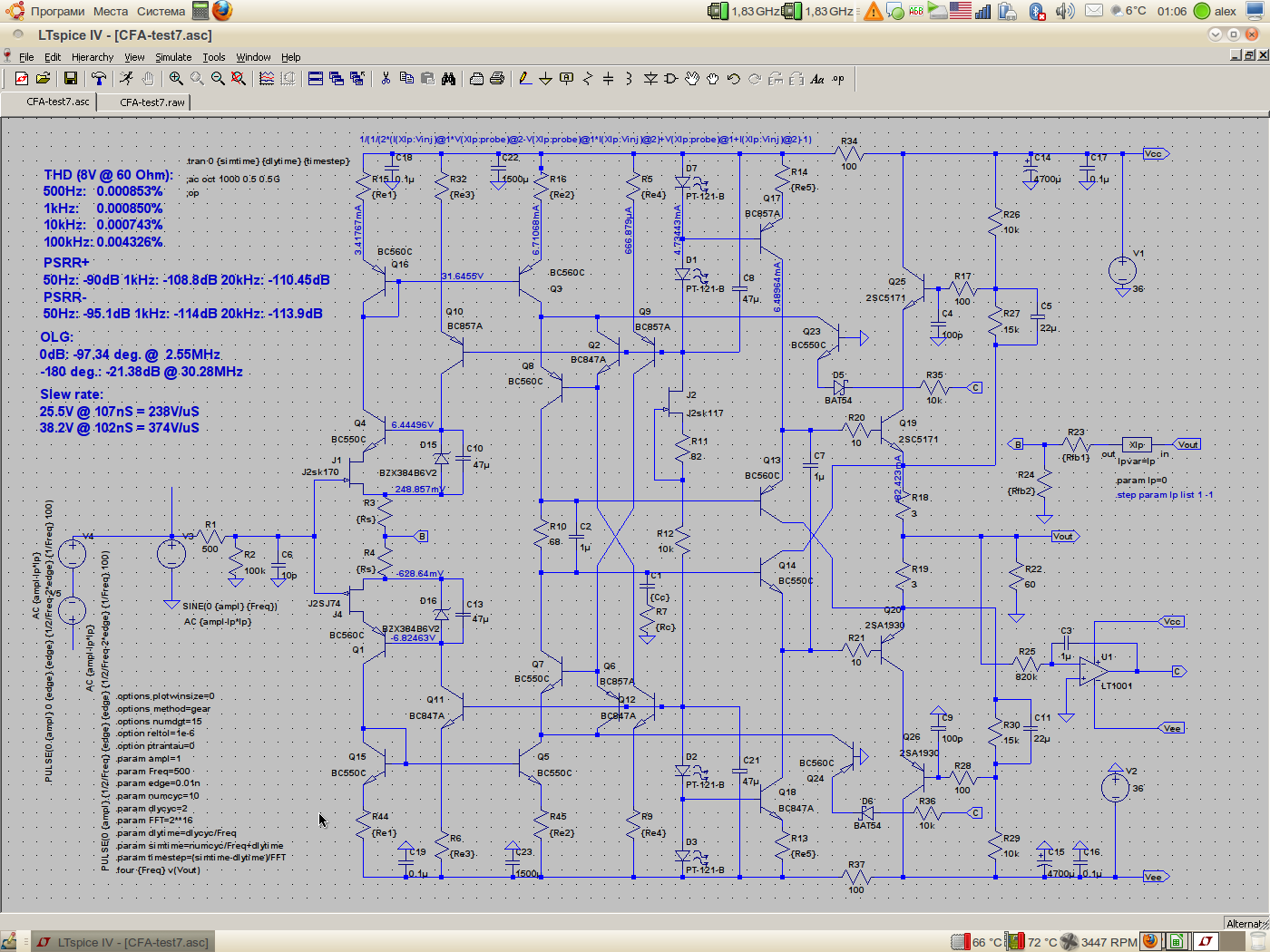
1. THD of the Diamond Buffer itself (without NFB) with 8V/1kHz input signal and 60 Ohm load is ~ 0.2%
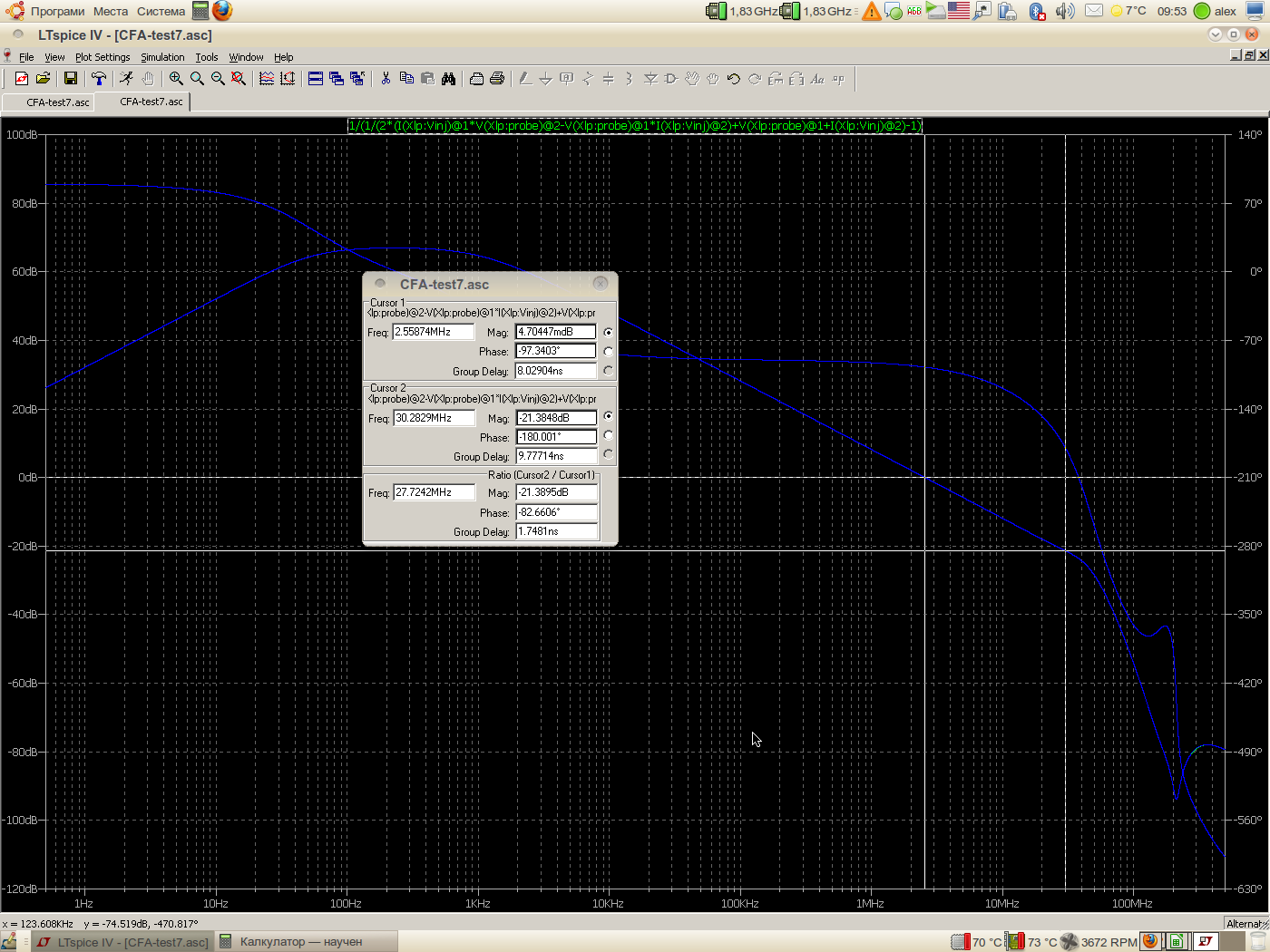
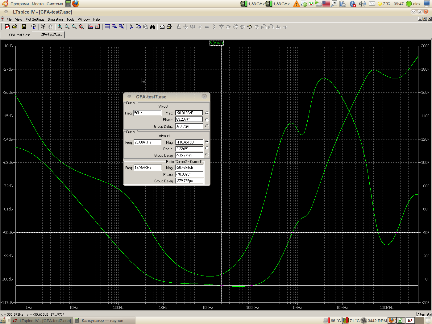
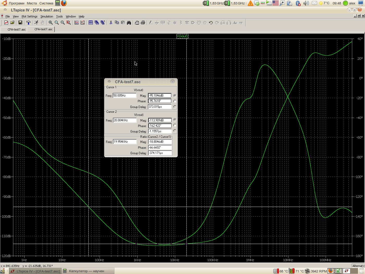
2. If we want to evaluate how buffer's THD vary with applied NFB loop gain we have to isolate it from the rest of schematic.
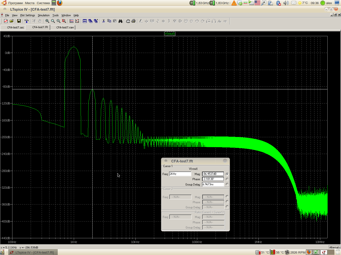
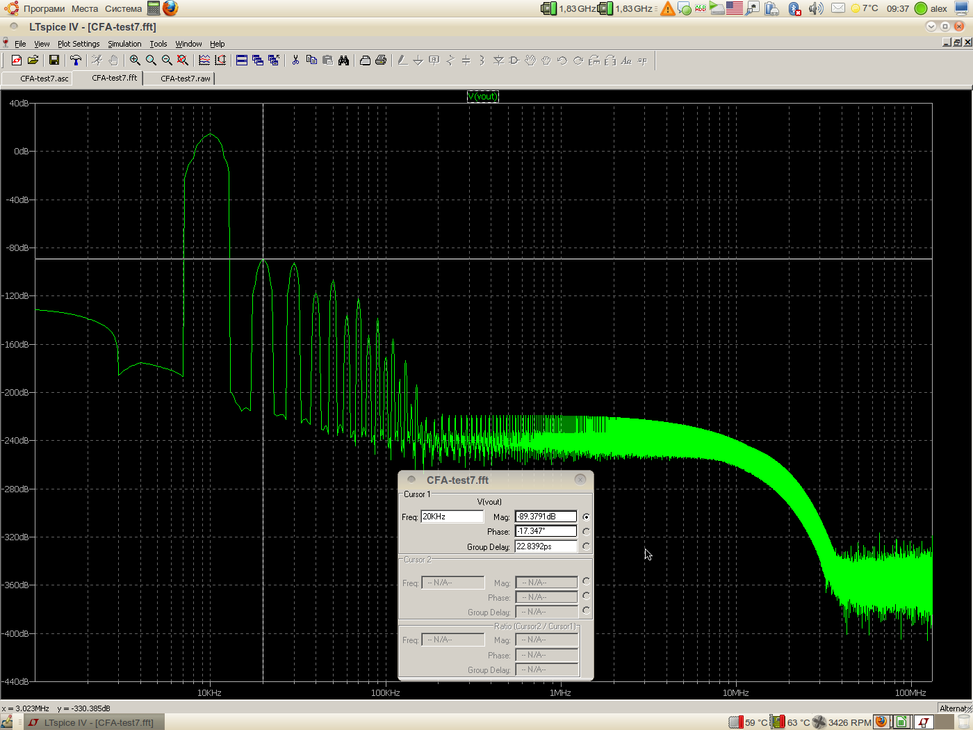
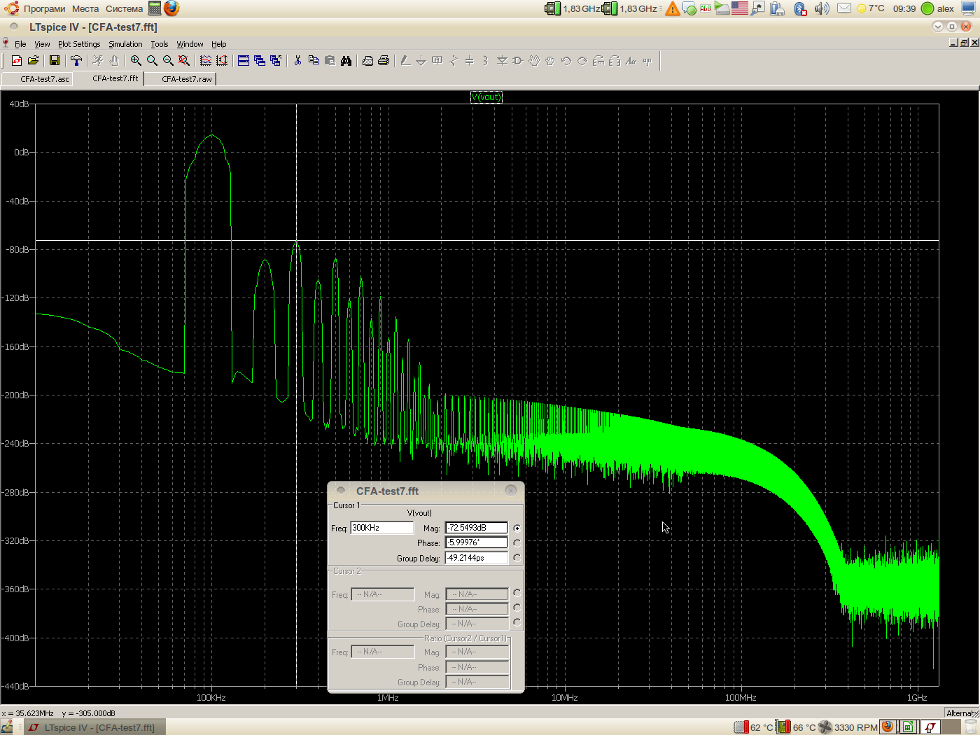
I did that and the results are shown on the picture:
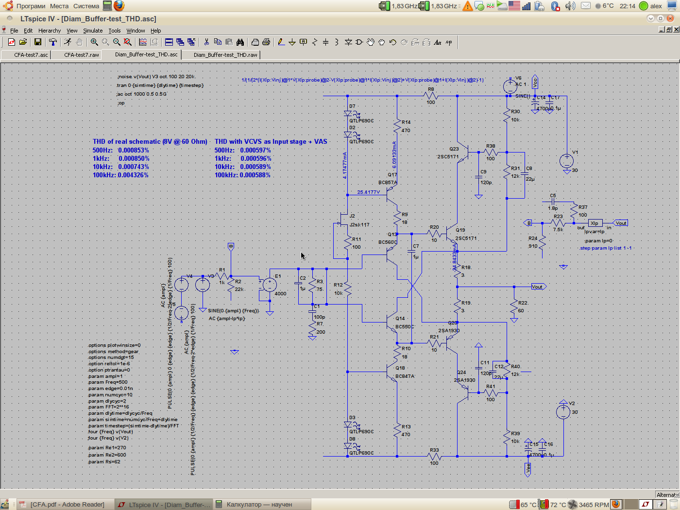
Input stage and VAS are substituted with ideal VCVS. Since the real schematic has OLG of aprox. 70dB, VCVS's amplification is set to 4000.
On the picture you can see calculated THDs with VCVS vs. these of the full schematic. It's obvious that they are very close (with exception of 100kHz measurements which is pretty normal). That's why I can say that it's almost all we can squeeze from schematic with 70dB OLG.
3. If we want to lower THDs, we must rise the OLG and hence the loop gain level. Do we really want this? I'm not sure. You can also ask John Curl about his opinion") .
.
4. About slew rate - I gave some values in the pictures above: 374V/us at 38.2V/100kHz output signal.
Regards
Alex
I'll try to answer you in several stages.
1. THD of the Diamond Buffer itself (without NFB) with 8V/1kHz input signal and 60 Ohm load is ~ 0.2%
2. If we want to evaluate how buffer's THD vary with applied NFB loop gain we have to isolate it from the rest of schematic.
I did that and the results are shown on the picture:
Input stage and VAS are substituted with ideal VCVS. Since the real schematic has OLG of aprox. 70dB, VCVS's amplification is set to 4000.
On the picture you can see calculated THDs with VCVS vs. these of the full schematic. It's obvious that they are very close (with exception of 100kHz measurements which is pretty normal). That's why I can say that it's almost all we can squeeze from schematic with 70dB OLG.
3. If we want to lower THDs, we must rise the OLG and hence the loop gain level. Do we really want this? I'm not sure. You can also ask John Curl about his opinion
.4. About slew rate - I gave some values in the pictures above: 374V/us at 38.2V/100kHz output signal.
Regards
Alex
Well, real schematic's THDs can be lowered even more by lowering the values of NFB resistors R23, R24 from 2.1k/300 Ohm to 620 and 142 Ohm respectively but amplifier will become a little bit unstable. So one can trade THD for stability.
Of course, I've already started to make the PCB but I suppose it will be ready at least in a week.
Regards
Alex
Of course, I've already started to make the PCB but I suppose it will be ready at least in a week.
Regards
Alex
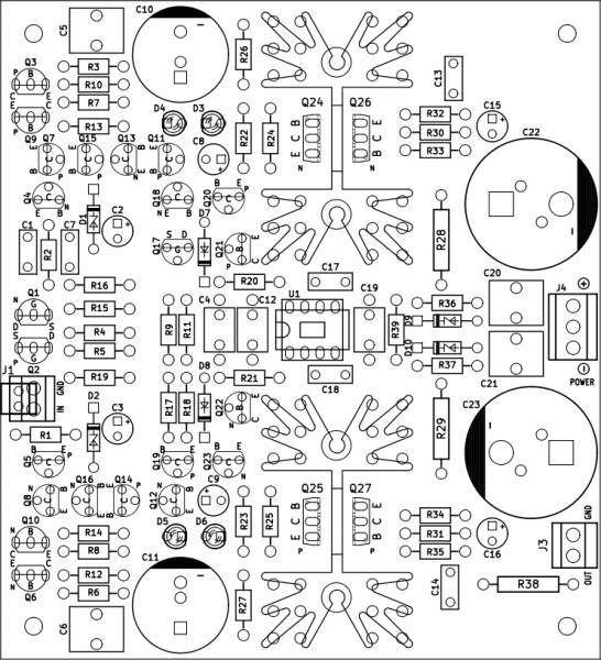
After almost an year delay and the populated PCBs from first version sent to a friend who "forgot" to send them back to me, I decided it's time for the second turn. I changed schematic a bit - the output is now with paralleled transistors (not driven cascode as in the previous version), the voltage sources for feeding the servo are different. A new PCB was designed and produced and here's results:
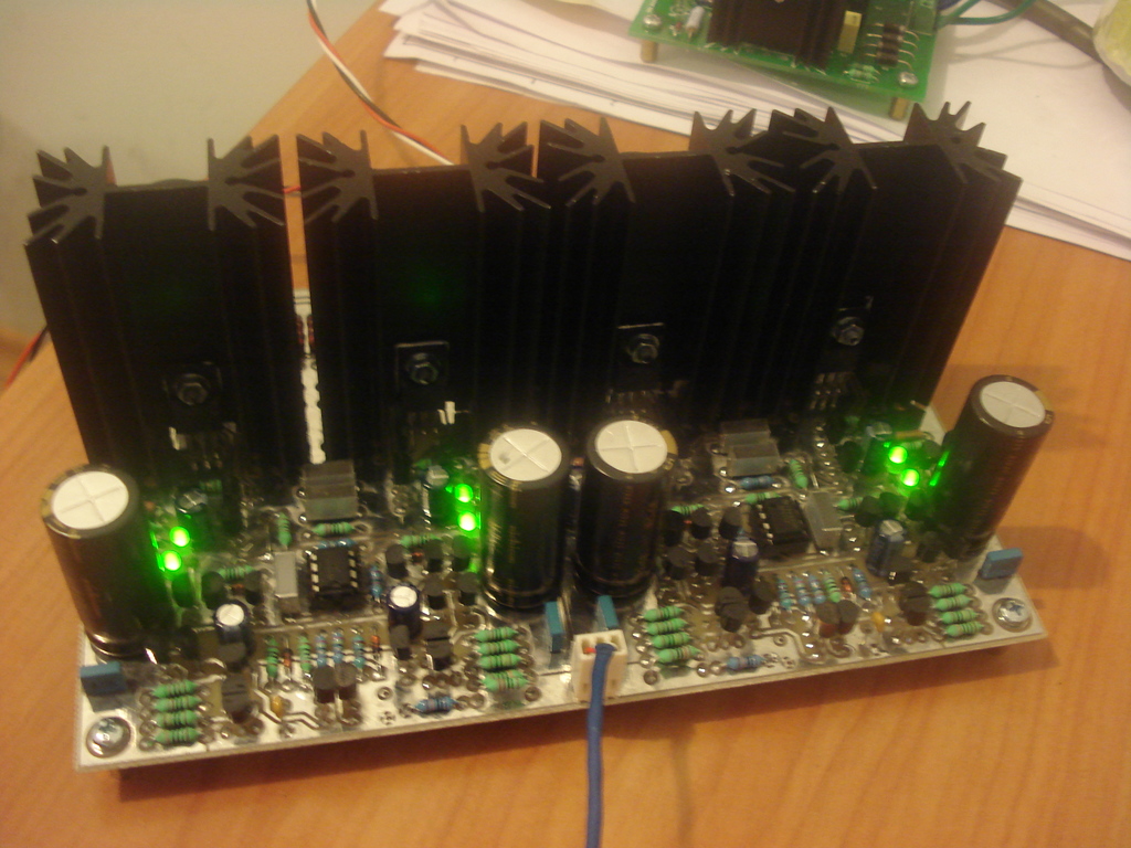
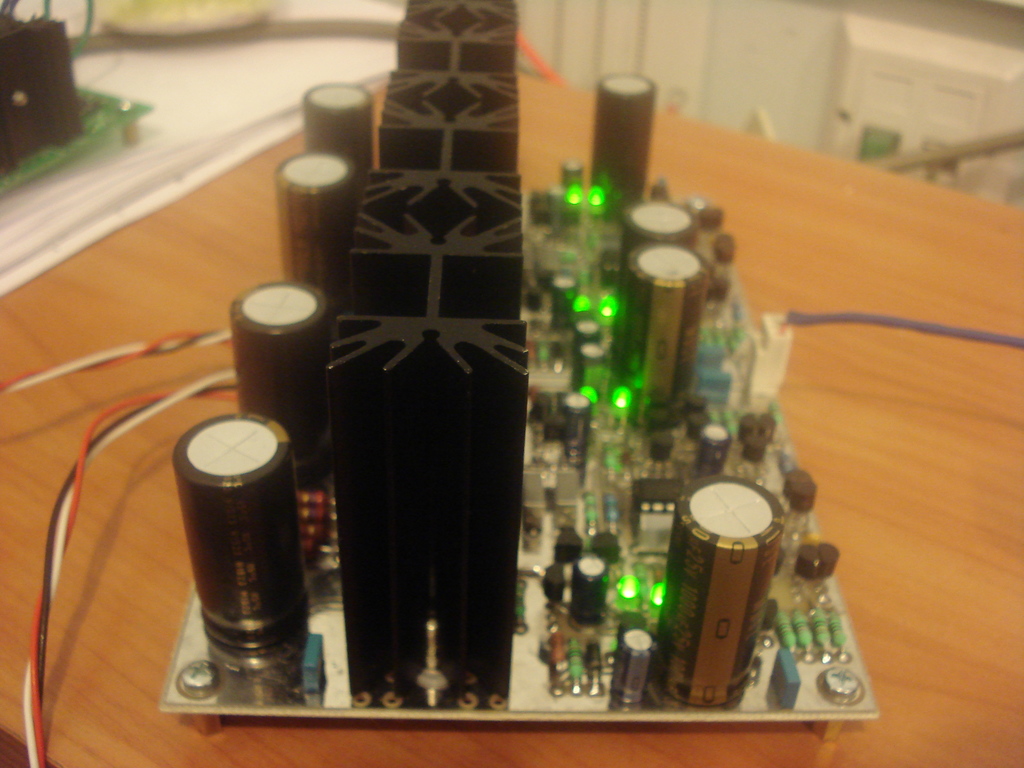
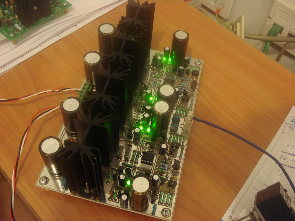
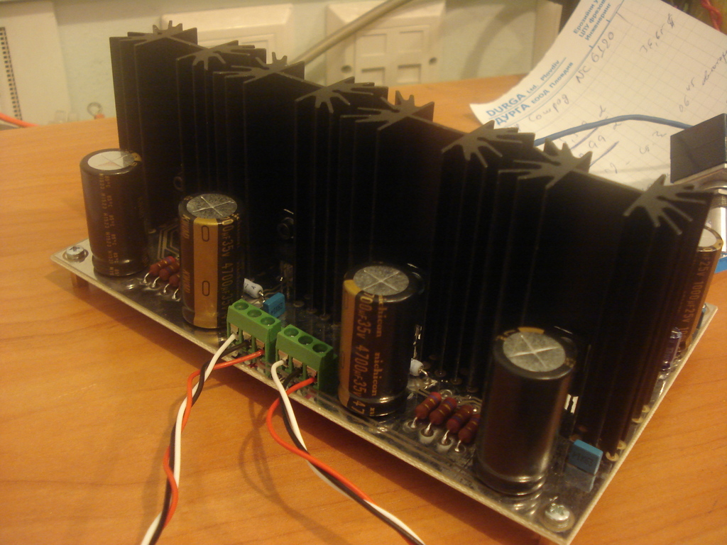
Power supply is +/- 24V regulated, the output transistors are biased at 70mA each.
There weren't any problems aliving schematic (nothing unexpected). After setting the DC modes I checked schematic's stability with 100kHz square wave signal. Simulated slew-rate was approx. 317 V/uS (20V rising edge for 63nS), the measured result is approx. 266 V/uS (20V rising edge for 75nS), which I think is not so bad at all. I didn't take the pictures from o'scope screen, but I'll do that soon. I haven't time for THD measurements yet - probably the next week.
Power supply is +/- 24V regulated, the output transistors are biased at 70mA each.
There weren't any problems aliving schematic (nothing unexpected). After setting the DC modes I checked schematic's stability with 100kHz square wave signal. Simulated slew-rate was approx. 317 V/uS (20V rising edge for 63nS), the measured result is approx. 266 V/uS (20V rising edge for 75nS), which I think is not so bad at all
. I didn't take the pictures from o'scope screen, but I'll do that soon. I haven't time for THD measurements yet - probably the next week.Oh, schematic, here it is:

I had a problems with stability and driven cascodes at the output. I tried various approaches and finally gave up - cut some traces and put transistors in parallel. For feeding the servo - this way it is independent of the PSU voltages and beside that we already have the zeners needed.
I had a problems with stability and driven cascodes at the output. I tried various approaches and finally gave up - cut some traces and put transistors in parallel. For feeding the servo - this way it is independent of the PSU voltages and beside that we already have the zeners needed
.And here's the promised picture of slew-rate measurement:
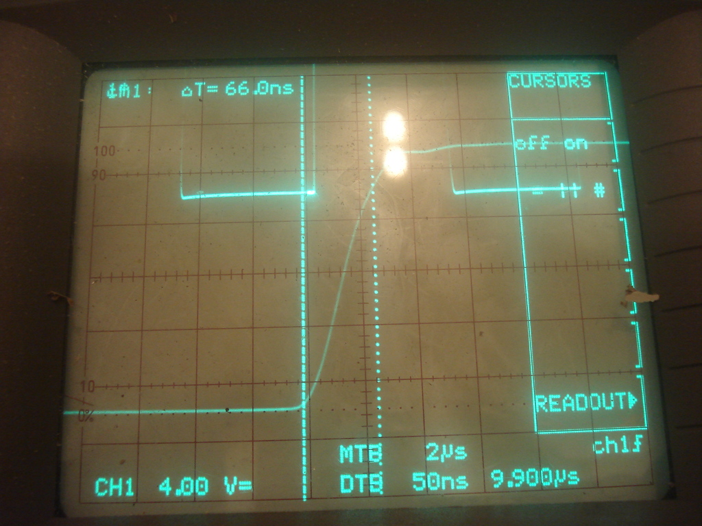
It's strange that cursors on the picture are shifted while I clearly remember that they were properly aligned on the scope screen. Nevermind it's obvious that the rising time is 66 nS which yields 242 V/uS for 16V swing.
It's strange that cursors on the picture are shifted while I clearly remember that they were properly aligned on the scope screen
. Nevermind it's obvious that the rising time is 66 nS which yields 242 V/uS for 16V swing.There are some very good HP amps around.... this one is amazing. A CFA, with high slew rate and ultra low distortion at any frequency and output level and load impedance.
I had a chance to measure it and here is an example --- 5KHz, 22 Ohm load, 3 v rms;

At a higher Freq and output voltage -- 10KHz, 5v rms and 8 Ohm load, the THD was just .01%
THx-RNMarsh
I had a chance to measure it and here is an example --- 5KHz, 22 Ohm load, 3 v rms;
At a higher Freq and output voltage -- 10KHz, 5v rms and 8 Ohm load, the THD was just .01%
THx-RNMarsh
Last edited:
- Home
- Amplifiers
- Headphone Systems
- CFA Headphones amplifier