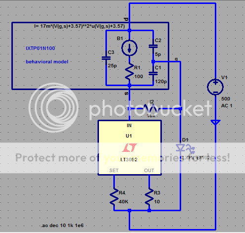
depletion mode enables two terminal floating ccs with more complex current regualtion if needed
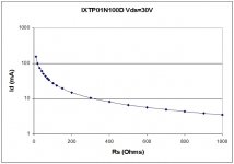
this simulated circuit is limited by Crss (~5 pF for IXTP01n100) |Z|> 1 MOhm @ 20 KHz
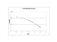
MOSFET model uses fit to measured gm points, datasheet C
IXTP0N100D measured curves
I prefer this device over the 10M45 or the DN2540. It has nice low Crss capacitance and really nice high -Vgs which makes it an excellent top-of-cascode device. A cascode of 2 of these has very high AC impedance and can be implemented with 2 MOSFETs and 3 resistors. IME, a single IXTP0N100 with 20V or more headroom has outstanding performance without needing to cascode.
My preference is also to use 2 terminal circuits as anode loads which allows N devices to be used (low capacitance, higher voltage ratings...)
Thanks for the pointer to the LT part. I was looking for a precise current source to use in a cascode, was trying to force fit a LT431!
Attachments
Last edited:
DN2540 with Neg voltage as Sink
current sink doubt.
I've used cascode DN2540 as CCsources with great success but now I'd like to know if I can use them as a SINK under the cathode and apply a HIGH NEGATIVE VOLTAGE. as an alternative to a 10M45 or alike.
So instead of sinking to ground I would apply a neg. voltage here for a direct coupling driver.
The DN2540 can handle up to +400 V I believe. Could I apply -300 volts under it pulling about 8 mA?
Would this work?
Yes, but you probably don't need anything like that much voltage for a long tail- all you need across the CCS is about 10V plus one half the expected peak signal voltage.
Thxs SY.
I was thinking if I had 210+ volts on the plate of a LTP and about -290 on the cathode adjustable and balanced, this would give me a fixed bias to the grid of the output tubes (adjustable -40- -85 volts with a trimmer).
Hence no coupling cap required.
Just an alternative to fixed bias supplies to each rail, requiring AC coupling.
Last edited:
An n-channel FET should work at least as well - maybe better as a current-sink (to negative, or to ground). The drain terminal maintains a high dynamic impedance by nature.
Running FETs too near the breakdown voltage is hazardous though. They are unforgiving to short overvoltage spikes. Think about what happens at switch-ON and -OFF, & measure the cathode voltage peaks!
Running FETs too near the breakdown voltage is hazardous though. They are unforgiving to short overvoltage spikes. Think about what happens at switch-ON and -OFF, & measure the cathode voltage peaks!
depletion mode enables two terminal floating ccs with more complex current regualtion if needed
this simulated circuit is limited by Crss (~5 pF for IXTP01n100) |Z|> 1 MOhm @ 20 KHz
MOSFET model uses fit to measured gm points, datasheet C
Can someone explain how the LXHL-BW02 is working? Is it as voltage limiter for the LT3092? Looking at the data sheet all I can see is that the Luxeon conducts 100mA at 3.1V with a nearly vertical curve to 350mA at 3.4V. No idea what the lower curve might look like.
Well, Ian, until the designer arrives to tell the tale, I'd say the LED is running a small current to Fix the FET gate at near to 3V. That will in turn run the source of a depletion FET a little higher: 4 to 5V [depending on FET and current level]. This gives the current source chip LT3092 a stable voltage environment to work in [ie cascode] and also prevents any startup transients from violating its 40V limit of durability.
I expect the designer intends R1 to be set such as not to limit the current unless there's a fault.
I expect the designer intends R1 to be set such as not to limit the current unless there's a fault.
Hey, Thanks Rod!
I figured he chose the Luxeon for a good reason and was hoping to find out what it was. (ie. why he chose it over any other LED or other kind of bias ref).
Not being spice literate I'll build it to see how it works so would like to understand more before picking parts.
I figured he chose the Luxeon for a good reason and was hoping to find out what it was. (ie. why he chose it over any other LED or other kind of bias ref).
Not being spice literate I'll build it to see how it works so would like to understand more before picking parts.
I expect the designer intends R1 to be set such as not to limit the current unless there's a fault.
Oh, I was thinking that R1,C1-3 were part of his LTspice model for the IXTP01n100. Is that not right?
You're right I think. The ON resistance of that FET at Vgs=0 is 80 ohms MAX, so it seems to be modelling for a slightly depleted Vgs. This could be hazardous if you attempt to simulate using different operating conditions. The Rds of a FET shows s lot of variation from sample to sample. Need the creator of the model to comment on the use of it really.
I have used ICs and opamps like this to make current sources for anode and filament circuits, and although they measure wonderfully, and have excellent stability, I just don't like the sound of them!
I have used ICs and opamps like this to make current sources for anode and filament circuits, and although they measure wonderfully, and have excellent stability, I just don't like the sound of them!
yes R1 is a internal part of a very quick and dirty model - at low currents as a ccs (or in my intended electrostatic headphone amp application) the Rds on isn't that important
the complete circuit hasn't been built - it is just a spice "sketch" to show how the parts could be strung together - there may be need for added gate stopper/"Zobel" to cut bandwidth and prevent oscillation
I have hooked up the IXTP cascoding simpler bjt ccs but only up to the 60 V limit of my lab supply so far
Last edited:
So far it has been more time efficient for me to build than try to model. For a few weeks now I've been running different versions of Salas' HV shunt reg and am surprised at how much small changes in the circuit's CCS had such substantial qualitative effects on sound. I've already tried casodes of DN2540 and IXTP01N100 and so far Salas' own single DMOS still sounds noticeably better.
Taking it as an opportunity to learn more about solid state devices I'm now on a hunt for recommended CCS circuits and thought I'd give jcx' one a try as it looks interesting and fresh (to my eyes anyway). My app sees B+ =300VDC , Vccs ~50V, Iccs 60mA (triode Ip =30mA / Ishunt `30mA). Do you think this circuit is worth trying here?
Taking it as an opportunity to learn more about solid state devices I'm now on a hunt for recommended CCS circuits and thought I'd give jcx' one a try as it looks interesting and fresh (to my eyes anyway). My app sees B+ =300VDC , Vccs ~50V, Iccs 60mA (triode Ip =30mA / Ishunt `30mA). Do you think this circuit is worth trying here?
Well, the simple DN2540 cascode that I use has 5 parts (the two FETs and three resistors), 100M source impedance and <12pA/rt Hz noise, so I'm not tempted to gild the lily.
Say, SY... 100M and 12pA/rt Hz, that means 1.2mV/rt Hz and 170mV over a 20kHz bandwidth, right?
That seems a lot, an average anode resistor only generates a few µV of noise under the same conditions?
Depends on the plate resistance since that's where the noise manifests. Let's take a triode-connected D3a, for example. The plate resistance is roughly 2k, so the noise voltage density generated is (12pA/rtHz)(2k) = 24nV/rtHz. Now, that's output-referred, so divide that by the gain (roughly 100) to get you to 0.24nV/rtHz, which is lost in the noise, so to speak, since it's uncorrelated with the tube's own Johnson noise.
- Status
- This old topic is closed. If you want to reopen this topic, contact a moderator using the "Report Post" button.
- Home
- Amplifiers
- Tubes / Valves
- CCS transistor choices