if you are using the same device in both channels then the transconductance will be within specification. That means at various Id the Yfs matches to within the tolerance specified.
Just pick two random mosFETs and a well designed circuit should swamp the variation in FET parameters. The little effect left over by varying parameters can be reduced by selecting devices. That first stage of selection is Vgs & Id the same (again within your measuring tolerances). If you want to go even further then you need to measure pairs of FETs each fed with the same Vgs and held at the same temperature and find some that pass the same ID. Now vary the Vgs a little either side of quiescent and see what pair still match for Id.
Just pick two random mosFETs and a well designed circuit should swamp the variation in FET parameters. The little effect left over by varying parameters can be reduced by selecting devices. That first stage of selection is Vgs & Id the same (again within your measuring tolerances). If you want to go even further then you need to measure pairs of FETs each fed with the same Vgs and held at the same temperature and find some that pass the same ID. Now vary the Vgs a little either side of quiescent and see what pair still match for Id.
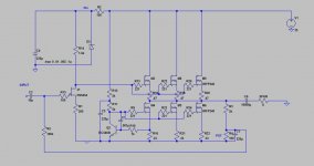
Well I've been fiddling a little more and have come up with the attached circuit as a possible fallback if the CCS input doesn't work out. The input has a set gain of 8x. Not sure how well it will work but it simms OK. It loses a little voltage swing due to the 33v zener but it's not too bad.
Going to lash up a few more CCS circuits now and take some measurements as I'm hoping I can keep the CCS input. Will keep you updated.
Oh, by the way, I'll only be running 2 pairs of output fets, not 3 as indicated on the diagram.
Going to lash up a few more CCS circuits now and take some measurements as I'm hoping I can keep the CCS input. Will keep you updated.
Oh, by the way, I'll only be running 2 pairs of output fets, not 3 as indicated on the diagram.
Attachments
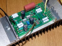
In the flesh....
Yes you're right. I think I'm going to stick to my original topology. Anyway, here it is in the flesh for testing....on much too small a heatsink") It's running pretty hot at 2 amps idle current per fet... have to run it in a shallow dish of water if I want it on for more than a minute. Final version will have a much larger heatsink...
It's running pretty hot at 2 amps idle current per fet... have to run it in a shallow dish of water if I want it on for more than a minute. Final version will have a much larger heatsink...
Having made this board I can now see how much space I wasted. Version 2 will be much neater and more compact.
Yes you're right. I think I'm going to stick to my original topology. Anyway, here it is in the flesh for testing....on much too small a heatsink
It's running pretty hot at 2 amps idle current per fet... have to run it in a shallow dish of water if I want it on for more than a minute. Final version will have a much larger heatsink...Having made this board I can now see how much space I wasted. Version 2 will be much neater and more compact.
Attachments
Last edited:
Some more pics...
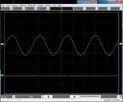
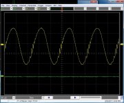
Attached are some scope shots. I have a nice clean wave at low power but as soon as I up it to over 15v p-p I get this nasty wave (figure 2). I think it might be caused by my bench top power supply running out of juice - its rated at 30v 5A, and I have it maxed out... can't test it until I build a new PS. I hope that's all it is.
Any thoughts?
Attachments
Hi,
Bias is set to 2A per device. Confirm.
Total bias is 6A. Confirm.
How can your 5A PSU supply a continuous 6A of bias current?
Test load is 8r0. Confirm.
Test voltage is 15Vpp = 7.5Vpk = ~5Vac Confirm.
Is the test load returned to ground or returned to +ve supply.
The current demand on the PSU is completely different for these two load return topologies.
Hi Andrew,
Thanks for your reply.
Bias is 2A per device, total bias is 4A (4 fets total)
Rail voltage = 30vdc.
Load = 7R.
Test voltage is as you determined (5VAC or thereabouts).
Speaker is returned to ground, though as you mentioned I should try returning it to v+ to ensure constant 4A current draw. That may solve my problem so I will give it a go.
Thanks again,
Greg.
7.5Vpk across 7r0 draws just over 1Apk.
The supply rail current will vary around 4A+-1A, i.e. from 2.93A to 5.07A even when the amplifier and the load are still working in ClassA.
Reduce your device bias to 1.5A and try again.
Reduce to 1A bias and try again.
Now move the load to the +ve rail and repeat all 3 experiments.
The supply rail current will vary around 4A+-1A, i.e. from 2.93A to 5.07A even when the amplifier and the load are still working in ClassA.
Reduce your device bias to 1.5A and try again.
Reduce to 1A bias and try again.
Now move the load to the +ve rail and repeat all 3 experiments.
Andrew,
Dropped the bias to 1A. Problem solved as expected.
Tried hooking the speaker from out to gnd and out to v+. I think the out to gnd had slightly better bass response, but difficult to tell with one channel and only using a 3" home theatre satellite speaker. Overall, difference did not appear to be substantial but unfortunately time between listening tests is fairly long due to the cumbersome setup, which makes solid comparisons difficult.
I ran a FFT analysis on the output. Distortion is very high, up around 10%. Going to give the circuit a go with a jfet front end and see if that improves anything. Still trying not to resort to global feedback at this stage.
Despite the high distortion it sounds quite nice. Mostly second harmonic. I think if it could get it down to a few percent I would be happy.
An interesting observation is that the output capacitor adds very little distortion (relative to the circuit itself). This has strengthened my wish to use an output capacitor for DC protection.
Thanks for your help so far. Will post back when I have made more progress.
Yes, SE produces increasing amounts of second harmonic as the output voltage approaches maximum.
If you are listening at average levels of <-20dB ref. maximum, i.e. max=25W and avg level is 200mW.
How often is the output within 10dB of maximum (>2.5W output) or within 3dB of maximum (>13W output)?
If you are listening at average levels of <-20dB ref. maximum, i.e. max=25W and avg level is 200mW.
How often is the output within 10dB of maximum (>2.5W output) or within 3dB of maximum (>13W output)?
- Status
- This old topic is closed. If you want to reopen this topic, contact a moderator using the "Report Post" button.
- Home
- Amplifiers
- Solid State
- Can I have some help with my class A amplifier design?