I have an issue with my Arcam Alpha 5. I was doing reclock:
- from clock X1 to saa7220 and 7310 (all good, CD is spinning TOC is read, play function is ok)
- from clock X/2 into TDA1541 pin2
- on the output there was music but hreavilly distorted
- I tried to do something also with pin4 of the TDA - originally this was connected to pin2 but I cut this link as found in some instructions and connected it to X1 of the clock
- since then nothing can be hear on the output; I checked and re-checked everything: voltages, frequencies etc. all look good to me. If I touch pin 6 or 25 (so the audio output) I can hear the brum so the audio path looks like is working.
- I completely removed 7220 and made everything NOS but still nothing on the output
did I fried the TDA? I'm not sure what kind of TDA was this: in the service manual it's written 1541 while everywhere on internet I found it's supposed to be 1541A. I can't read the chip as I have some silicone paste with an aluminium radiator on top of it (previously, sound was distorted immediately after TDA was getting a bit warmer - so there was already something going on with that chip)
Thanks
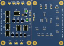
Hi Guys,
Attached is a 3D render of a PCB ive been working on based on ecdesigns schematics #6315
Design consists of 4 layers with 1 and 4 for traces, 2 and 3 for GND and VCC. Reg is a LP5907 3.3V.
If this works as it should then I think this will be a cost effective solution for diyers. The only difficult bit for diyers will be soldering the SMD parts which have a pitch of 1.27mm (50 mils). If its an issue I may be able to help out.
Thanks to ecdesigns for sharing his circuits to help out us diyers.
Attachments
Hi Ryan,
This is good job, but have you considered reclocking the LE output from a low-jitter master clock? It is just one more D-type flip-flop instead of U11. I am afraid of increased jitter of the timing critical LE going through all this logic circuitry.
This is good job, but have you considered reclocking the LE output from a low-jitter master clock? It is just one more D-type flip-flop instead of U11. I am afraid of increased jitter of the timing critical LE going through all this logic circuitry.
Last edited:
Hi Ryan,
This is good job, but have you considered reclocking the LE output from a low-jitter master clock? It is just one more D-type flip-flop instead of U11. I am afraid of increased jitter of the timing critical LE going through all this logic circuitry.
Hi Icsaszar,
Yes the thought crossed my mind, although I would like to keep Johns circuit the way it is and use it how he intended it to be used for now. When I get behind the wheel of circuit design and let my creativity loose is when things can go a little pear shaped.
Maybe I could rearrange a few things on the PCB to get LE as far away as possible from the rest of the circuitry, some via stitching alongside the LE trace perhaps.
Would you consider adding option of through hole solder pads for your input/outputs?
Hi Guys,
Attached is a 3D render of a PCB ive been working on based on ecdesigns schematics #6315
Design consists of 4 layers with 1 and 4 for traces, 2 and 3 for GND and VCC. Reg is a LP5907 3.3V.
If this works as it should then I think this will be a cost effective solution for diyers. The only difficult bit for diyers will be soldering the SMD parts which have a pitch of 1.27mm (50 mils). If its an issue I may be able to help out.
Thanks to ecdesigns for sharing his circuits to help out us diyers.
Would you consider adding option of through hole solder pads for your input/outputs?
Hi sthcoaster,
I might be able to sort something out, I'll get it all working first and then finalize the design.
Anyone interested in this board please send me a message so I can get an idea on numbers. Thanks.
Would you consider this a "lo-tech" alternative to the whole fifo, i2stopcm business?I would like to try simultaneous but the iancanada route confuses me and feels like an expensive addition
This is what I want to find out, I'm really interested how this will sound against Ians I2S to PCM PCB. Ians board uses a software code to convert the signal, Johns uses only logic gates so will be an interesting comparison. I dont think I would consider it lo-tech, just a different approach but worth trying.
I'll be testing Johns circuit with and without Ians FIFO before it.
As I mentioned before, this board will be a much more cost effective way to convert input modes.
Last edited by a moderator:
Hi Icsaszar,
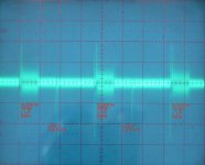
When you study how this circuit operates you would see that this is a non-issue.
The TDA1541A interface is completely shut down well before and after output latching (attached oscillogram). So the interference generated by the decoder becomes moot as this oscillogram shows. That's the whole point, avoiding problems instead of attempting to fix these afterwards.
Timing jitter is usually not causing audible changes in the sound, as long as jitter stays within reasonable limits, say within 100ps ... 400ps.
The related varying spectrum and demodulation products cause the -clearly audible- differences even with minute changes in jitter amplitude and or spectrum. Tackle this spectrum and you fix the -audible- jitter problem.
From what I know right now, crystal oscillators should not be used in or anywhere near a DAC because of related issues with modulated carrier and peak in the spectrum (fundamental).
In many devices, spread spectrum clocks have to be used in order to avoid peaks in the spectrum and to be able to meet emc directives.
This is good job, but have you considered reclocking the LE output from a low-jitter master clock? It is just one more D-type flip-flop instead of U11. I am afraid of increased jitter of the timing critical LE going through all this logic circuitry.
When you study how this circuit operates you would see that this is a non-issue.
The TDA1541A interface is completely shut down well before and after output latching (attached oscillogram). So the interference generated by the decoder becomes moot as this oscillogram shows. That's the whole point, avoiding problems instead of attempting to fix these afterwards.
Timing jitter is usually not causing audible changes in the sound, as long as jitter stays within reasonable limits, say within 100ps ... 400ps.
The related varying spectrum and demodulation products cause the -clearly audible- differences even with minute changes in jitter amplitude and or spectrum. Tackle this spectrum and you fix the -audible- jitter problem.
From what I know right now, crystal oscillators should not be used in or anywhere near a DAC because of related issues with modulated carrier and peak in the spectrum (fundamental).
In many devices, spread spectrum clocks have to be used in order to avoid peaks in the spectrum and to be able to meet emc directives.
Attachments
Hello Ryan,
Greetings from Germany to Australia. You have made a nice PCB out of the circuit. I am still working on a TDA1541A DAC. So I am interested in your PCB.
Have a nice day.
Regards
André
Hi André,
Ok ill take note of that and keep you informed of my progress.
Thanks.
The board looks fine, a nice addition would be two inverters for those who want to use it for a dual differential setup.Ians board uses a software code to convert the signal, Johns uses only logic gates so will be an interesting comparison. I dont think I would consider it lo-tech, just a different approach but worth trying.
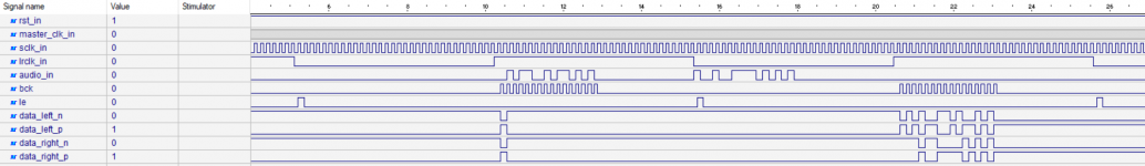
I'm taking the CPLD route (still logic gates, no software based conversion
") ) I just finished the VHDL-code which implements the logic gates on the CPLD. The picture shows the simulation of this code.
) I just finished the VHDL-code which implements the logic gates on the CPLD. The picture shows the simulation of this code.Attachments
The board looks fine, a nice addition would be two inverters for those who want to use it for a dual differential setup.
I'm taking the CPLD route (still logic gates, no software based conversion
Hi knuisje,
Not a bad idea, but I dont think ill go down the balanced road. Although im curious how the Signed Magnitude idea for the 1541 will sound. I might attempt this sometime soon.
Hi.I attached a schematic diagram of an I2S to Simultaneous converter for the TDA1541A.
The circuit performs following functions:
- Identify and invert MSB within the serial data stream.
- Delay the left channel data in order to align it with the R channel data.
- Create a 16 bit window for clock and data output signals.
Timing diagram is added at the bottom.
The circuit can be built with logic building blocks like 74HC, 74 AHC, 74LV, 74LVC.
If U13 is a problem one can combine two 74HC86 XOR gates instead. One output goes to one input of the other XOR gate, we now have an XOR gate with 3 inputs and one output. The 74LVC1G386 is available in SOT32-6 housing:
http://www.ti.com/lit/ds/symlink/sn74lvc1g386.pdf
Depending on logic building block properties the circuit can work on voltages between 2V4 and 5V. I recommend to use 2V4 ... 3V3 supply voltage.
Connections:
I2S,
DI = D
WSI = WS
BCKI = BCK
Simultaneous,
OB/TWC (pin 27) connects to -5V to put the TDA1541A in simultaneous mode.
DOL connects to pin 3
DOR connects to pin 4
BCKO connects to pin 2
LE connects to pin 1
LE determines the exact moment of output latching, output latching occurs at the 0 -> 1 transition (TDA1541A set to simultaneous mode).
BCK clocks in the data on the 1 -> 0 transition (TDA1541A set to simultaneous mode).
Couldn´t this (as well as the i2s to signed magnitude described earlier) be used with TDA1543? Of course using two 1543 for each 1541 and only take the analog signal from one channel in each of the 1543. As far as I recall, one of the dac´s in the 1543 is performing slightly better than the other, but I do not remember witch. Is this so?
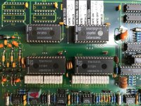
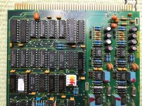
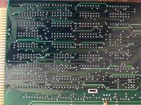
I've seen a lot of pics of tda1541a in situ. But not this one.
Recently, I won an online auction for 4 X boards pulled from a working AMS Audiofile, ie. one of the original HD recorders for studio production. Each board has 2x SAA7220P/B and 2 x TDA1541A (all early 90s production). I paid less than £40 for the lot (ie. 8x TDA1541A) - lucky me.
Surprisingly online search reveals very little. I have asked AMS for service manual but they politely declined; they don't provide manuals/schematics even for legacy items as old as this. Can anybody here help? Nothing on Hifiengine either.
The reason for this post is the large number of logic gates and other devices including *4HC you can see on the board. Could this be some kind of implementation similar to ecdesigns recent suggestion? I'm trying to trace where these all connect to the tda1541.
Recently, I won an online auction for 4 X boards pulled from a working AMS Audiofile, ie. one of the original HD recorders for studio production. Each board has 2x SAA7220P/B and 2 x TDA1541A (all early 90s production). I paid less than £40
for the lot (ie. 8x TDA1541A) - lucky me.Surprisingly online search reveals very little. I have asked AMS for service manual but they politely declined; they don't provide manuals/schematics even for legacy items as old as this. Can anybody here help? Nothing on Hifiengine either.
The reason for this post is the large number of logic gates and other devices including *4HC you can see on the board. Could this be some kind of implementation similar to ecdesigns recent suggestion? I'm trying to trace where these all connect to the tda1541.
Attachments
Hi Ryan,
I am interested in your I2S to SIMULTANEOUS PCB.
Regards
Nick
Ok, noted.
If anyone else is interested just send me a PM to keep this thread unpolluted.
Thanks.
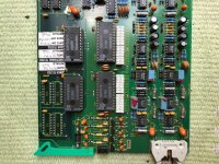
Found this I2S to simultaneous board on eBay - using logic gates by the looks
I2s to Simultaneous Converter for tda1540 DAC or tda1541 and tda1541a | eBay
I2s to Simultaneous Converter for tda1540 DAC or tda1541 and tda1541a | eBay
- Home
- Source & Line
- Digital Line Level
- Building the ultimate NOS DAC using TDA1541A