SSerg: there is no need to have any correlation between the oscillator frequency and sampling frequency. This is why there are the 7x large filter capacitors at the current divider pins. Different if you omit the filter capacitors, then you need integer number of DEM cycles within a sampling period (I tried this approach, also sounds good, but smaller "DEM clock" steps are superimposed on the output signal steps).
At low DEM clock frequency (50 Hz) one has to use large filter capacitors, and I am worrying about leakage current of electrolytics. I tried tantalums before, but they were very microphonic.
At low DEM clock frequency (50 Hz) one has to use large filter capacitors, and I am worrying about leakage current of electrolytics. I tried tantalums before, but they were very microphonic.
SSerg: there is no need to have any correlation between the oscillator frequency and sampling frequency.
This is a controversial statement. If you read the monograph Rudy van de Plassche about the DEM method, it becomes clear that for each sample, the currents of the active divider should be averaged by alternating them. Otherwise, the accuracy of the current division will not correspond to the claimed (10 ^ -5).
And the samples follow with a frequency of 44 kHz at least.
The DEM-circuit was designed from the perspective to be able to compensate every conversion individually (44.1K/s in NOS and 176.4K/s oversampled) in order to achieve greater over-all accuracy. Which you can read in the datasheet of the TDA1540 where the principles of operation are described.SSerg: there is no need to have any correlation between the oscillator frequency and sampling frequency. This is why there are the 7x large filter capacitors at the current divider pins. Different if you omit the filter capacitors, then you need integer number of DEM cycles within a sampling period (I tried this approach, also sounds good, but smaller "DEM clock" steps are superimposed on the output signal steps).
At low DEM clock frequency (50 Hz) one has to use large filter capacitors, and I am worrying about leakage current of electrolytics. I tried tantalums before, but they were very microphonic.
Using a 50 Hz DEM frequency does not have the accuarcy of the individual conversions in mind but acts on an "average" of which the validity is not confirmed.
Hi SSerg,
DEM is required for averaging between 4 bit currents that have minor tolerances (matching of elements on the chip). It's all explained in the document that Alexandre posted. The goal is obtaining good matching bit currents from a circuit that has known tolerances.
In order to average between 4 slightly different bit currents, each corrected bit output current should represent the AVERAGE of all 4 input bit currents that have slight tolerances.
Suppose we have following INPUT bit currents:
Input bit current #1, 0.98mA
Input bit current #2, 0.92mA
Input bit current #3, 1.00mA
Input bit current #4, 0.90mA
And we use a switch matrix to connect each INPUT bit current to each output for 25% of a full DEM cycle:
25% of 0.98 + 25% of 0.92 + 25% of 1.00 + 25% of 0.90 = 0.95mA (output bit current #1)
25% of 0.92 + 25% of 1.00 + 25% of 0.90 + 25% of 0.98 = 0.95mA (output bit current #2)
25% of 1.00 + 25% of 0.92 + 25% of 1.00 + 25% of 0.90 = 0.95mA (output bit current #3)
25% of 0.90 + 25% of 0.98 + 25% of 0.92 + 25% of 1.00 = 0.95mA (output bit current #3)
Now we get 4 bit currents that have the same AVERAGE value, but with a ripple current that depends on the element matching:
Poor matching -> High ripple current.
Perfect matching -> No ripple current.
Since nothing is perfect there will be some ripple current and it is minimised by the active divider decoupling (lowpass filter) cap. The value of the filter cap is inverse proportional with the DEM frequency:
Low DEM frequency -> Big (high value) filter cap.
High DEM frequency -> Small (low value) filter cap.
All I did is reduce the DEM frequency, this will obviously lower the ripple current frequency too, so I simply used bigger (larger value) caps to take care of the lower ripple frequency, that's all.
There is no reason whatsoever why this averaging circuit would suddenly no longer work only because the switching frequency is changed.
If I would switch with 1Hz, it would now take 4 seconds to complete one DEM cycle and we would need Big electrolytic capacitors to filter out the 1 Hz ripple current.
If we would switch 1 million times a second, it would take 4us to complete one DEM cycle and we would only need a small capacitor to filter out the ripple current.
However, when increasing DEM clock rate we also increase the number of ground-bounces / second.
With 50Hz DEM I only have 50 ground-bounces / second. With 44.1 KHz sample rate this translates to one ground-bounce every 882 samples (no problem whatsoever).
With 1 MHz DEM I have 1 million ground-bounces a second. With 44.1 KHz sample rate this translates to 22.6 ground bounces WITHIN one sample.
The DEM switch matrix isn't perfect, the switches have finite switching time and each switch has tolerances in propagation time. At higher switch frequencies parasitics also start to play a major role.
The lower the DEM frequency, the lower the impact of switch timing tolerances on the generated average bit current.
With 50Hz DEM frequency, timing tolerances in DEM switches have virtually zero impact on accuracy. Bit accuracy is as high as it gets.
With 1 MHz DEM frequency, timing tolerances in the DEM switches and parasitics play a big role in bit accuracy. Bit accuracy will be poor, that's why Philips advised to use a DEM frequency that's not higher than roughly 200 KHz.
Knowing Philips they would have used 2MHz DEM clock and 10nF decoupling caps if this didn't cause any degrading as this saves cost (10nF caps are cheaper then 100nF caps).
Similar Philips would not have used lower DEM frequency because this requires bigger (more expensive) decoupling caps.
Finally, because there is on-chip crosstalk, DEM frequencies WITHIN the audio spectrum would become audible as very weak idle tones (I tested this). With 50Hz DEM I am at the low end of the audio spectrum and with this low DEM clock rate crosstalk is negligible as we only have one ground-bounce after every 882 samples.
Ground-bounce also leads to trigger uncertainty, so it is desirable to have fewest (preferably zero) ground-bounces the moment the TDA1541A outputs are latched. This gives lowest on-chip jitter.
--->>>> I included oscillograms of my prototype running on 50Hz DEM frequency in a previous post that prove that low level performance is superb, this would simply be impossible when DEM was not working perfectly. I left the DAC playing for a few days and re-tested low level performance, still perfect. Now you have some explaining to do")
As explained this is not a very good idea. Many of us (me included) had moments where a distorted signal seemed to sound better to the ears.
This 50-KHz DEM generator castrate the very idea of DEM, since the currents of the active divider do not alternate within one sample. But John does not pay attention to this. He believes that it is more important to ensure low switching noise. With the same success you can just shut the DEM generator.
DEM is required for averaging between 4 bit currents that have minor tolerances (matching of elements on the chip). It's all explained in the document that Alexandre posted. The goal is obtaining good matching bit currents from a circuit that has known tolerances.
In order to average between 4 slightly different bit currents, each corrected bit output current should represent the AVERAGE of all 4 input bit currents that have slight tolerances.
Suppose we have following INPUT bit currents:
Input bit current #1, 0.98mA
Input bit current #2, 0.92mA
Input bit current #3, 1.00mA
Input bit current #4, 0.90mA
And we use a switch matrix to connect each INPUT bit current to each output for 25% of a full DEM cycle:
25% of 0.98 + 25% of 0.92 + 25% of 1.00 + 25% of 0.90 = 0.95mA (output bit current #1)
25% of 0.92 + 25% of 1.00 + 25% of 0.90 + 25% of 0.98 = 0.95mA (output bit current #2)
25% of 1.00 + 25% of 0.92 + 25% of 1.00 + 25% of 0.90 = 0.95mA (output bit current #3)
25% of 0.90 + 25% of 0.98 + 25% of 0.92 + 25% of 1.00 = 0.95mA (output bit current #3)
Now we get 4 bit currents that have the same AVERAGE value, but with a ripple current that depends on the element matching:
Poor matching -> High ripple current.
Perfect matching -> No ripple current.
Since nothing is perfect there will be some ripple current and it is minimised by the active divider decoupling (lowpass filter) cap. The value of the filter cap is inverse proportional with the DEM frequency:
Low DEM frequency -> Big (high value) filter cap.
High DEM frequency -> Small (low value) filter cap.
All I did is reduce the DEM frequency, this will obviously lower the ripple current frequency too, so I simply used bigger (larger value) caps to take care of the lower ripple frequency, that's all.
There is no reason whatsoever why this averaging circuit would suddenly no longer work only because the switching frequency is changed.
If I would switch with 1Hz, it would now take 4 seconds to complete one DEM cycle and we would need Big electrolytic capacitors to filter out the 1 Hz ripple current.
If we would switch 1 million times a second, it would take 4us to complete one DEM cycle and we would only need a small capacitor to filter out the ripple current.
However, when increasing DEM clock rate we also increase the number of ground-bounces / second.
With 50Hz DEM I only have 50 ground-bounces / second. With 44.1 KHz sample rate this translates to one ground-bounce every 882 samples (no problem whatsoever).
With 1 MHz DEM I have 1 million ground-bounces a second. With 44.1 KHz sample rate this translates to 22.6 ground bounces WITHIN one sample.
The DEM switch matrix isn't perfect, the switches have finite switching time and each switch has tolerances in propagation time. At higher switch frequencies parasitics also start to play a major role.
The lower the DEM frequency, the lower the impact of switch timing tolerances on the generated average bit current.
With 50Hz DEM frequency, timing tolerances in DEM switches have virtually zero impact on accuracy. Bit accuracy is as high as it gets.
With 1 MHz DEM frequency, timing tolerances in the DEM switches and parasitics play a big role in bit accuracy. Bit accuracy will be poor, that's why Philips advised to use a DEM frequency that's not higher than roughly 200 KHz.
Knowing Philips they would have used 2MHz DEM clock and 10nF decoupling caps if this didn't cause any degrading as this saves cost (10nF caps are cheaper then 100nF caps).
Similar Philips would not have used lower DEM frequency because this requires bigger (more expensive) decoupling caps.
Finally, because there is on-chip crosstalk, DEM frequencies WITHIN the audio spectrum would become audible as very weak idle tones (I tested this). With 50Hz DEM I am at the low end of the audio spectrum and with this low DEM clock rate crosstalk is negligible as we only have one ground-bounce after every 882 samples.
Ground-bounce also leads to trigger uncertainty, so it is desirable to have fewest (preferably zero) ground-bounces the moment the TDA1541A outputs are latched. This gives lowest on-chip jitter.
--->>>> I included oscillograms of my prototype running on 50Hz DEM frequency in a previous post that prove that low level performance is superb, this would simply be impossible when DEM was not working perfectly. I left the DAC playing for a few days and re-tested low level performance, still perfect. Now you have some explaining to do
In my estimation, the oscillator frequency should be of the order of 700-800 kHz. This frequency should be selected by ear.
As explained this is not a very good idea. Many of us (me included) had moments where a distorted signal seemed to sound better to the ears.
Hi John,
Exactly. But this averaging should be done for EACH sample, i.e. within each sampling period equal to 1/44100 sec. Therefore, it is not possible to reduce the frequency of alternating bit currents with impunity, this will result in the loss of the accuracy of the D/A conversion.
And in my post I had in mind of course 50 Hz, and not 50 kHz.
In order to average between 4 slightly different bit currents, each corrected bit output current should represent the AVERAGE of all 4 input bit currents that have slight tolerances.
Exactly. But this averaging should be done for EACH sample, i.e. within each sampling period equal to 1/44100 sec. Therefore, it is not possible to reduce the frequency of alternating bit currents with impunity, this will result in the loss of the accuracy of the D/A conversion.
And in my post I had in mind of course 50 Hz, and not 50 kHz.
Hello John,
you wrote that for decoupling you use:
>Decoupling caps, 14 x 100uF/25V Nichicon UKA, plus connected to GND. DEM >oscillator timing cap 1uF/50V WIMA r=2.5mm. Bias resistor 12K 1% between pins 15 >and 17.
dvb projekt recommends SMD decoupling caps in his BOM:
>If you could solder SMD, use the Cornell Dubilier 1µF/16V FCA 1210 caps
Is there any significant difference between caps apart from the used space?
Thanks,
xaled
TDA1541's DEM is rather different than modern DEMs, their ripple is smoothed each current segments' decoup pins. So, if ripple is able to be ignored, it is seen as precise binary weighted voltage references and V/I converters(a resister and cascode transistor), isn't it? If it is, in such ideal case, I think 50Hz DEM freq is OK.
Hi John,
Yesterday there was no time, sorry. Today, I read your post to the end.
So please provide the spectrum at a signal level of 0 dB and -60 dB (1 kHz) for a 50Hz DEM. It would be nice to compare analogous spectra for 200kHz DEM (700kHz?).
Yesterday there was no time, sorry. Today, I read your post to the end.
You are right, ears are sometimes deceived.Now you have some explaining to do
Many of us (me included) had moments where a distorted signal seemed to sound better to the ears.
So please provide the spectrum at a signal level of 0 dB and -60 dB (1 kHz) for a 50Hz DEM. It would be nice to compare analogous spectra for 200kHz DEM (700kHz?).
Hi weissi,
Ground-bounce is a known issue with all chips, modern chips included.
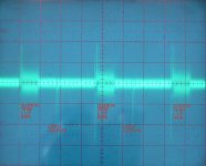
I attached an oscillogram showing TDA1541A (simultaneous interface) on-chip ground-bounce that leaks to its outputs. vertical setting 2mV/div, probe 1:1. BCK and data signals have 1K series resistor to slow down the edges, LE has 33R series resistor. Drive level of the digital interface signals equals 2V4pp.
We see ground-bounce during clocking in L + R data and one single bounce during output latching with the LE signal (using the TDA1541A in simultaneous mode).
We can clearly see that ground-bounce has reached zero when we issue the LE impulse that is highly critical for sample timing.
Average switching noise is reduced by 75% as we only have digital interface activity during 16 of the 64 bits in a frame.
Full scale output voltage equals 560mVpp, one LSB represents 8.5uV. The ground-bounce amplitude equals 2mV! see why it is important to reduce switching noise?
With say 5.65Vpp full scale output I measured roughly 20mVpp on the active I/V converter output. LSB now corresponds with 86uV.
We can't solve the on-chip ground-bounce, circuits have to switch and circuits have parasitic capacitances that need to be charged and discharged. This in turn pulls local ground up and pushes local ground down while the parasitic capacitance is being charged and discharged.
But what about following, if we use two TDA1541A chips and feed the second chip with BCK and data signals that are exactly 0.5 bit delayed like this:
_______----------_______----------________ BCK chip 1
----------_______----------_______----------- BCK chip 2
____________________________________
--------------------|-------------------|--------- DATA chip 1
___________________________________
----------|-------------------|------------------ DATA chip 2
Then combine the outputs of both chips (segmented structure for example). Now a positive bounce on chip 1 output will coincide with a negative bounce on the chip 2 output.
+ plus - gives 0 and - plus + gives 0. So we can attenuate, possibly almost cancel the switching noise on the TDA1541A combined output.
This could also work for DEM, but both DEM clocks would have to run in perfect sync and DEM for chip 2 needs to be delayed by exactly half a DEM period:
----------------------___________________-------------------- DEM chip 1
________________--------------------------_______________DEM chip 2
By using low frequency (50Hz DEM) for both chips there would be no problem and we can simply use two free running 50Hz DEM clocks.
BCK can be delayed by 0.5 bit by inverting it.
DATA can be delayed by 0.5 bit by using a D flip-flip that is clocked by the non inverted BCK signal, we already did this in the protocol converter circuit.
Do you think that Philips engineers where aware of that ground bounce? I could imagine using multiple bonds from one GND pin to the die would have improved that alot. Anyway, something that can't be solved.
Ground-bounce is a known issue with all chips, modern chips included.
I attached an oscillogram showing TDA1541A (simultaneous interface) on-chip ground-bounce that leaks to its outputs. vertical setting 2mV/div, probe 1:1. BCK and data signals have 1K series resistor to slow down the edges, LE has 33R series resistor. Drive level of the digital interface signals equals 2V4pp.
We see ground-bounce during clocking in L + R data and one single bounce during output latching with the LE signal (using the TDA1541A in simultaneous mode).
We can clearly see that ground-bounce has reached zero when we issue the LE impulse that is highly critical for sample timing.
Average switching noise is reduced by 75% as we only have digital interface activity during 16 of the 64 bits in a frame.
Full scale output voltage equals 560mVpp, one LSB represents 8.5uV. The ground-bounce amplitude equals 2mV! see why it is important to reduce switching noise?
With say 5.65Vpp full scale output I measured roughly 20mVpp on the active I/V converter output. LSB now corresponds with 86uV.
We can't solve the on-chip ground-bounce, circuits have to switch and circuits have parasitic capacitances that need to be charged and discharged. This in turn pulls local ground up and pushes local ground down while the parasitic capacitance is being charged and discharged.
But what about following, if we use two TDA1541A chips and feed the second chip with BCK and data signals that are exactly 0.5 bit delayed like this:
_______----------_______----------________ BCK chip 1
----------_______----------_______----------- BCK chip 2
____________________________________
--------------------|-------------------|--------- DATA chip 1
___________________________________
----------|-------------------|------------------ DATA chip 2
Then combine the outputs of both chips (segmented structure for example). Now a positive bounce on chip 1 output will coincide with a negative bounce on the chip 2 output.
+ plus - gives 0 and - plus + gives 0. So we can attenuate, possibly almost cancel the switching noise on the TDA1541A combined output.
This could also work for DEM, but both DEM clocks would have to run in perfect sync and DEM for chip 2 needs to be delayed by exactly half a DEM period:
----------------------___________________-------------------- DEM chip 1
________________--------------------------_______________DEM chip 2
By using low frequency (50Hz DEM) for both chips there would be no problem and we can simply use two free running 50Hz DEM clocks.
BCK can be delayed by 0.5 bit by inverting it.
DATA can be delayed by 0.5 bit by using a D flip-flip that is clocked by the non inverted BCK signal, we already did this in the protocol converter circuit.
Attachments
Hi xaled,
Yes of course, 100nF ... 1uF decoupling cap is fine with 250 KHz DEM clock (470 ... 680pF timing cap).
But I experimented with 50Hz DEM clock (1uF timing cap).
This results in much lower ripple frequency (50Hz instead of 250 KHz) so I have to increase the value of the decoupling caps to approx. 100uF/25V (6mm diameter) in order to maintain low ripple current. I kept increasing the capacitor value until measurements no longer revealed any significant ripple, this is how I arrived at 100uF.
The voltage rating is also important. When operating electrolytic capacitors close to the voltage rating, DC leakage current increases.
When connecting a 16V cap to 30V supply, DC leakage current increases to the point the capacitor heats up, produces gasses and the safety vent is deformed or pops open.
We have roughly -13V average on the decoupling pins, that's why I chose 25V rating (for low DC leakage current).
Because I use low (50Hz) DEM frequency the RF decoupling issues have vanished and we can now use longer traces and larger size caps while maintaining good decoupling.
Hello John,
you wrote that for decoupling you use:
>Decoupling caps, 14 x 100uF/25V Nichicon UKA, plus connected to GND. DEM >oscillator timing cap 1uF/50V WIMA r=2.5mm. Bias resistor 12K 1% between pins 15 >and 17.
dvb projekt recommends SMD decoupling caps in his BOM:
>If you could solder SMD, use the Cornell Dubilier 1µF/16V FCA 1210 caps
Is there any significant difference between caps apart from the used space?
Thanks,
xaled
Yes of course, 100nF ... 1uF decoupling cap is fine with 250 KHz DEM clock (470 ... 680pF timing cap).
But I experimented with 50Hz DEM clock (1uF timing cap).
This results in much lower ripple frequency (50Hz instead of 250 KHz) so I have to increase the value of the decoupling caps to approx. 100uF/25V (6mm diameter) in order to maintain low ripple current. I kept increasing the capacitor value until measurements no longer revealed any significant ripple, this is how I arrived at 100uF.
The voltage rating is also important. When operating electrolytic capacitors close to the voltage rating, DC leakage current increases.
When connecting a 16V cap to 30V supply, DC leakage current increases to the point the capacitor heats up, produces gasses and the safety vent is deformed or pops open.
We have roughly -13V average on the decoupling pins, that's why I chose 25V rating (for low DC leakage current).
Because I use low (50Hz) DEM frequency the RF decoupling issues have vanished and we can now use longer traces and larger size caps while maintaining good decoupling.
Because I use low (50Hz) DEM frequency the RF decoupling issues have vanished and we can now use longer traces and larger size caps while maintaining good decoupling.
Dear -EC-,
Could adding local inductance help reduce ground bounce even further?
If tantalum caps are microphonic, as some mate commented, some sort of mechanical damping could be used...
Cheers,
M.
Hi SSerg,
TDA1541A in Philips CD player (4 times oversampling).
DEM clock runs on roughly 250 KHz (16us to complete one cycle) Sample rate 44.1 * 4 = 176.4 KHz. (5.6us)
It is -impossible- to complete a DEM cycle as you suggested, as it takes 16us to complete while a sample lasts only 5.6us
TDA1541A in Sony CD player (8 times oversampling).
DEM clock runs on roughly 250 KHz (16us to complete one cycle) Sample rate 44.1 * 4 = 352.8 KHz. (2.83us)
It is -impossible- to complete a DEM cycle as you suggested as it takes 16us to complete while a sample lasts only 2.83us
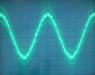
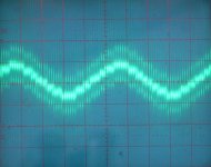
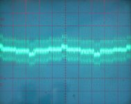
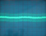
I attached oscillograms of low level measurements with the TDA1541A (plain A) in 17 bits (102dB range) segmented (signed magnitude) mode. This DAC runs on a 50Hz DEM with 100uF/25V decoupling caps. The slightest errors in the 6 MSB currents and low level performance is lost instantly.
Oscillogram 1, 1 KHz, -70dB (11.7 bit range).
Oscillogram 2, 1 KHz, -80dB (13.3 bit range).
Oscillogram 3, 1 KHz, -90dB (15 bit range).
Oscillogram 4, 1 KHz, -100dB (16.7 bit range).
So where exactly does DEM go wrong? I can resolve 17 bits using plain A chips, DEM cycle takes 80ms (80,000us) to complete while sample period time equals 22.6us (44.1 KHz NOS).
The biggest problem is digital interface related switching noise, it's all over the oscillograms.
With the "Aikido" drive method (segments driven with 0.5bit delay) I might possibly fix that too.
What matters most of all is how a DAC responds to a bombardement of sine wave signals (music). Simple 1 KHz -100 ... 0dB test signal would never reveal any of this.
We have interface signals (clock & data) that have direct impact on chip performance, modulated carrier waves are created and demodulated, injection locking, injection pulling effects you name it.
Focussing on the TDA1541A DEM clock we have a carrier frequency of say 250KHz that is FM modulated with the incoming data pattern. The 2 x 6K8 or 1 x 12K bias resistor greatly reduces this effect but it's still there. Please observe DEM frequency with or without music being streamed. With 250 Khz DEM we planted a FM radio transmitter in our DAC chip that transmits the (I2S) data pattern.
Curious how this distortion sounds after demodulating? connect a pair of headphones to the I2S data signal using a series resistor. This is what I personally don't want to have in the DAC output signal. When you increase the DEM clock frequency, the modulated carrier frequency can reach circuits even more easily (given parasitic capacitances) making matters much worse.
By using 50Hz DEM clock I simply do not create a modulated RF carrier frequency and I do not get all related problems.
-60dB sine wave on a poor performing DAC would sound like a weak clean sine wave suggesting all is fine.
Play a piano or violin recording on that same DAC and things can go very wrong.
Therefore DACs need to be tested with large number of digital audio files that address each and every possible flaw in a DAC. THD tests are fine for verifying basic functionality and locating errors but that's about it.
Exactly. But this averaging should be done for EACH sample, i.e. within each sampling period equal to 1/44100 sec. Therefore, it is not possible to reduce the frequency of alternating bit currents with impunity, this will result in the loss of the accuracy of the D/A conversion.
TDA1541A in Philips CD player (4 times oversampling).
DEM clock runs on roughly 250 KHz (16us to complete one cycle) Sample rate 44.1 * 4 = 176.4 KHz. (5.6us)
It is -impossible- to complete a DEM cycle as you suggested, as it takes 16us to complete while a sample lasts only 5.6us
TDA1541A in Sony CD player (8 times oversampling).
DEM clock runs on roughly 250 KHz (16us to complete one cycle) Sample rate 44.1 * 4 = 352.8 KHz. (2.83us)
It is -impossible- to complete a DEM cycle as you suggested as it takes 16us to complete while a sample lasts only 2.83us
I attached oscillograms of low level measurements with the TDA1541A (plain A) in 17 bits (102dB range) segmented (signed magnitude) mode. This DAC runs on a 50Hz DEM with 100uF/25V decoupling caps. The slightest errors in the 6 MSB currents and low level performance is lost instantly.
Oscillogram 1, 1 KHz, -70dB (11.7 bit range).
Oscillogram 2, 1 KHz, -80dB (13.3 bit range).
Oscillogram 3, 1 KHz, -90dB (15 bit range).
Oscillogram 4, 1 KHz, -100dB (16.7 bit range).
So where exactly does DEM go wrong? I can resolve 17 bits using plain A chips, DEM cycle takes 80ms (80,000us) to complete while sample period time equals 22.6us (44.1 KHz NOS).
The biggest problem is digital interface related switching noise, it's all over the oscillograms.
With the "Aikido" drive method (segments driven with 0.5bit delay) I might possibly fix that too.
It would be nice to compare analogous spectra for 200kHz DEM (700kHz?).
What matters most of all is how a DAC responds to a bombardement of sine wave signals (music). Simple 1 KHz -100 ... 0dB test signal would never reveal any of this.
We have interface signals (clock & data) that have direct impact on chip performance, modulated carrier waves are created and demodulated, injection locking, injection pulling effects you name it.
Focussing on the TDA1541A DEM clock we have a carrier frequency of say 250KHz that is FM modulated with the incoming data pattern. The 2 x 6K8 or 1 x 12K bias resistor greatly reduces this effect but it's still there. Please observe DEM frequency with or without music being streamed. With 250 Khz DEM we planted a FM radio transmitter in our DAC chip that transmits the (I2S) data pattern.
Curious how this distortion sounds after demodulating? connect a pair of headphones to the I2S data signal using a series resistor. This is what I personally don't want to have in the DAC output signal. When you increase the DEM clock frequency, the modulated carrier frequency can reach circuits even more easily (given parasitic capacitances) making matters much worse.
By using 50Hz DEM clock I simply do not create a modulated RF carrier frequency and I do not get all related problems.
-60dB sine wave on a poor performing DAC would sound like a weak clean sine wave suggesting all is fine.
Play a piano or violin recording on that same DAC and things can go very wrong.
Therefore DACs need to be tested with large number of digital audio files that address each and every possible flaw in a DAC. THD tests are fine for verifying basic functionality and locating errors but that's about it.
Attachments
Hi EC,
When running at a 50hz DEM - Would it be possible to use a lower value than 100uF for the LSB ripple filter caps? Theoretically, the LSB would only need only a few uF correct?
For your latest 1541A scheme, you have set up your current bias above the output current of AOL/AOR giving a positive voltage bias on the outputs, have you found any benefits in doing this? I remember you saying a while back that you measured lower distortion when the voltage on the outputs where around -45mV.
I tried your solution to the current offset and used a plain old resistor instead of a CCS and the result was as you described, less graininess, and less fatigue.
And thanks for taking the time to explain everything in so much detail - I finally understand the workings of the current dividers and the DEM, that thesis paper posted a few pages back helped a lot too.
Ryan
Last edited:
Thank you, John, for the measurements given.
It can be seen from them that the 1541 responds confidently to the signal at the level of -80 dB. True, the sinusoid turned into a triangular saw.
It seems to me that you confuse two things: the resolving power of conversion and the accuracy of conversion. If the DAC has responded to a weak signal, this does not mean that this response is accurate.
To estimate the accuracy of the conversion, it is necessary to watch the frequency spectrum of the output signal. On it we will see the products of distortions caused by the nonlinearity of the transformation.
To estimate the accuracy of the conversion, it is necessary to watch the frequency spectrum of the output signal. On it we will see the products of distortions caused by the nonlinearity of the transformation.
The output spectrum makes it possible to give a comprehensive assessment of the quality of the conversion, taking into account various interference and distortions.
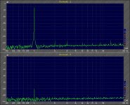
In order to understand what is meant, I give an example of the output spectrum from my DAC to TDA1541 (signal level -10 dB full scale).
Where are your spectra, John?
So where exactly does DEM go wrong? I can resolve 17 bits using plain A chips
It can be seen from them that the 1541 responds confidently to the signal at the level of -80 dB. True, the sinusoid turned into a triangular saw.
It seems to me that you confuse two things: the resolving power of conversion and the accuracy of conversion. If the DAC has responded to a weak signal, this does not mean that this response is accurate.
To estimate the accuracy of the conversion, it is necessary to watch the frequency spectrum of the output signal. On it we will see the products of distortions caused by the nonlinearity of the transformation.
To estimate the accuracy of the conversion, it is necessary to watch the frequency spectrum of the output signal. On it we will see the products of distortions caused by the nonlinearity of the transformation.
The output spectrum makes it possible to give a comprehensive assessment of the quality of the conversion, taking into account various interference and distortions.
In order to understand what is meant, I give an example of the output spectrum from my DAC to TDA1541 (signal level -10 dB full scale).
Where are your spectra, John?
Attachments
Hi weissi,
Classical I/U cascade on the opamp (AD842); the feedback resistor, if I recall correctly, is 1.3K.SSerg - what kind of I/V are you using? Thx, Markus
Very promising, I can see this helping with the BCK superimposed noise, which seems to be dominant (looking at the oscillograms).
What about synchronous DEM clock, at a low frequency? One could try 86.13 Hz, 172.26 Hz, 344.53 Hz.
Thanks John!
Then combine the outputs of both chips (segmented structure for example). Now a positive bounce on chip 1 output will coincide with a negative bounce on the chip 2 output.
+ plus - gives 0 and - plus + gives 0. So we can attenuate, possibly almost cancel the switching noise on the TDA1541A combined output.
This could also work for DEM, but both DEM clocks would have to run in perfect sync and DEM for chip 2 needs to be delayed by exactly half a DEM period
What about synchronous DEM clock, at a low frequency? One could try 86.13 Hz, 172.26 Hz, 344.53 Hz.
Thanks John!
- Home
- Source & Line
- Digital Line Level
- Building the ultimate NOS DAC using TDA1541A