15VA Green Square 15W Sealed toroidal transformers M15-04 AC dual 15V(2*15V) | eBay
I have this transformer and it reads 18.8V is this normal?
hi,
if it is measured without load, you have a regulation of about 18%, so the ac voltage without load is minimum 17,7V AC. you also have to add the AC variation of the primary side.
BR
Günni
Those are very interesting developments for the TDA1541.
I used the passive I/V and tube stage for the PCM56K dual cd player and never find it acceptable. You could hear the sound change with a cathode follower output tube.
Now that I built 3 tda1541 boards, 1 is a disaster, 2 has still issues and was placed in NOS which I don't like. However I have a feedback active I/V transistor design which I obtained and it is good to use, please see the link here: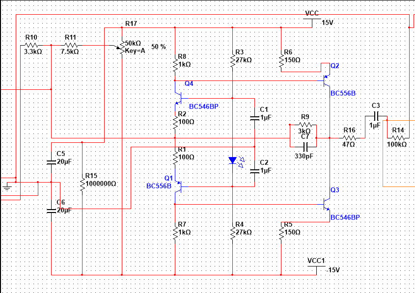
Thanks John for the info.
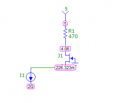
I will certainly try this super simple I/V, with digital volume control. With 2SK170-BL. There will always be enough current on the JFET if using digital volume. For example there will be 1mA if a peak reaches -6dBFS (this will rarely occur).
The current source I1 is just a representation of the DAC chip. Just connect the JFET source to the output pin of TDA1541, nothing else.
The advantage is constant current draw on the regulators, lower apparent R seen by the DAC (on the order of 40 ohms) and a slightly larger I/V resistor possible. The +5 is the signal ground now.
Since the output pin of TDA1541 can swing slightly more towards the positive than the negative without protection diodes conducting, the 200mV is no issue, it is actually closer to the "center" than 0V.
I tested -many- active I/V converters and none of these offered satisfying results.
I will certainly try this super simple I/V, with digital volume control. With 2SK170-BL. There will always be enough current on the JFET if using digital volume. For example there will be 1mA if a peak reaches -6dBFS (this will rarely occur).
The current source I1 is just a representation of the DAC chip. Just connect the JFET source to the output pin of TDA1541, nothing else.
The advantage is constant current draw on the regulators, lower apparent R seen by the DAC (on the order of 40 ohms) and a slightly larger I/V resistor possible. The +5 is the signal ground now.
Since the output pin of TDA1541 can swing slightly more towards the positive than the negative without protection diodes conducting, the 200mV is no issue, it is actually closer to the "center" than 0V.
Attachments
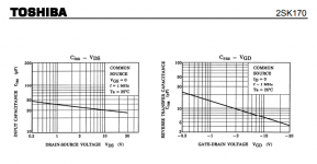
Even though the capacitances between source pin and grounded gate (roughly equal to Ciss below) and between drain and grounded gate (equal to Crss below) are variable (with signal), I believe their -3dB cut points will be well into the MHz range in this application. It certainly simultates a quite high bandwidth.
Attachments
Final remarks. This is for use with digital volume only. Where the signal will rarely, or never, exceed -6dBFS. The signal ground is +5. Taken right from the terminals of the I/V resistor in an actual implementation. You don´t want to use 0V as your signal ground because the regulator+decoupling combo becomes your coupling capacitor.
Last edited:
The DEM oscillator runs at approx. 50Hz. I use a 1uF film timing cap for this.
The 12K DEM bias resistor minimises jitter and improves stability when data is streaming.
Dear John,
With DEM being of much interest to many.
With R5 = 12k as drawn, how is this different from pins 16, 17 to -15V via 6k8
Rgz,
Hanze.
Thanks John for the info.
I will certainly try this super simple I/V, with digital volume control. With 2SK170-BL. There will always be enough current on the JFET if using digital volume. For example there will be 1mA if a peak reaches -6dBFS (this will rarely occur).
The current source I1 is just a representation of the DAC chip. Just connect the JFET source to the output pin of TDA1541, nothing else.
The advantage is constant current draw on the regulators, lower apparent R seen by the DAC (on the order of 40 ohms) and a slightly larger I/V resistor possible. The +5 is the signal ground now.
Since the output pin of TDA1541 can swing slightly more towards the positive than the negative without protection diodes conducting, the 200mV is no issue, it is actually closer to the "center" than 0V.
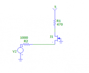
I suggest a small current of say 1 mA minimum to - 5 V to ensure the fet remains on at all times (class A) to prevent pinching.
- I did this with a SMD-MOSFET 2SK1078 and it worked very good. My resistor at the top was 1k5 (the well known value) and my V+ was slightly higher (200 V to be precise, I cascoded with a tube) and the NOS steps were immaculate.
- The only thing I did wrong was that I did not have a diode (BAT?) from out to earth. So at start up with a cold tube the TDA output saw -5V. It ruined my TDA1541A . .
You may be right. See below, the fet gate is now tied to the true signal ground (+5V) by means of the 100nF cap, and it is possible to set the source to 0V, or slightly more if it gives a better result (the "center" for lowest distortion seems to be a bit above 0V).
The bias resistor suggested by triode_al is not needed if you are using digital volume control. For me the worst case signal peak would be -6dBFS or less, which leaves more than 1mA for the fet to operate (it doesn´t get close to pinch off).
Hmmm, turn on conditions have to be evaluated... triode_al said he ruined his tda1541 during turn on.
Thanks
Alex
Attachments
John, can you explain the reason for lowering the DEM clock to such a low frequency. Perhaps you've already explained and I've missed it. But I'm also interested into the theory behind this move.....
The DEM oscillator runs at approx. 50Hz. I use a 1uF film timing cap for this.
The 12K DEM bias resistor minimises jitter and improves stability when data is streaming. The datasheet DEM oscillator works excellent when no data is streamed but runs into -big- troubles (jitter, instability) when the data stream starts. The 12K DEM bias resistor fixes this problem.
The DEM clock is still free running as with the datasheet application.
Actually, I had no problem understanding you raising the frequency earlier in this thread. It was in line with the theoretical workings of the DEM circuit and an intended application by the TDA1541A's designers. So going the complete other way puzzles me.
Thanks in advance,
Edwin
Hi esgigt,
There is significant on-chip crosstalk between the DEM circuit, digital audio interface and the generated audio signal.
With given stray capacitance, crosstalk increases with increasing frequency. So it is essential to use lowest practical switching frequencies regardless of the DAC chip.
I also measured increasing low level distortion with increasing DEM frequency. I tested 20 KHz, 200KHz, 2 MHz and 6.4 MHz.
The 200KHz DEM switching frequency gets phase / frequency modulated when the audio stream is started (on-chip crosstalk changes the DEM oscillator frequency). This effect can be greatly reduced with the bias resistor I added.
Now we have a 200 KHz radio transmitter inside the TDA1541A that transmits interference (data switching noise spectrum). This causes distortion that cannot be removed or filtered out. Even when using huge decoupling caps, the wireless on-chip interference would remain.
Even worse, when attempting to decouple 200KHz radio frequency, the PCB lay-out and decoupling caps become highly critical. In practice decoupling won't be very effective given the long traces (including the wire frame leads inside the large TDA1541A chip).
200KHz DEM also causes permanent on-chip ground-bounce that promotes on-chip trigger uncertainty and related on-chip jitter.
The most logical thing to do is to lower the DEM frequency to say 50Hz so crosstalk is greatly reduced and the 200KHz interference broadcasting station is shut down. Other advantage is that 50Hz mains hum will fully mask the related very weak 50Hz DEM clock idle tones.
The consequence is that we need bigger decoupling caps (100uF) as the switching frequency is reduced from 200 KHz to 50Hz. Ripple measurements on the decoupling pins and low level signal tests lead to this practical value of 100uF.
It is possible to lower the DEM frequency even further to 5Hz, for example using 1000uF decoupling caps.
This does not improve things any further and 1000uF takes a long time to charge with the bit currents (5 ... 10 minutes before the bit currents have settled). The 5 Hz DEM frequency won't be masked by 50Hz hum either.
John, can you explain the reason for lowering the DEM clock to such a low frequency. Perhaps you've already explained and I've missed it. But I'm also interested into the theory behind this move.
There is significant on-chip crosstalk between the DEM circuit, digital audio interface and the generated audio signal.
With given stray capacitance, crosstalk increases with increasing frequency. So it is essential to use lowest practical switching frequencies regardless of the DAC chip.
I also measured increasing low level distortion with increasing DEM frequency. I tested 20 KHz, 200KHz, 2 MHz and 6.4 MHz.
The 200KHz DEM switching frequency gets phase / frequency modulated when the audio stream is started (on-chip crosstalk changes the DEM oscillator frequency). This effect can be greatly reduced with the bias resistor I added.
Now we have a 200 KHz radio transmitter inside the TDA1541A that transmits interference (data switching noise spectrum). This causes distortion that cannot be removed or filtered out. Even when using huge decoupling caps, the wireless on-chip interference would remain.
Even worse, when attempting to decouple 200KHz radio frequency, the PCB lay-out and decoupling caps become highly critical. In practice decoupling won't be very effective given the long traces (including the wire frame leads inside the large TDA1541A chip).
200KHz DEM also causes permanent on-chip ground-bounce that promotes on-chip trigger uncertainty and related on-chip jitter.
The most logical thing to do is to lower the DEM frequency to say 50Hz so crosstalk is greatly reduced and the 200KHz interference broadcasting station is shut down. Other advantage is that 50Hz mains hum will fully mask the related very weak 50Hz DEM clock idle tones.
The consequence is that we need bigger decoupling caps (100uF) as the switching frequency is reduced from 200 KHz to 50Hz. Ripple measurements on the decoupling pins and low level signal tests lead to this practical value of 100uF.
It is possible to lower the DEM frequency even further to 5Hz, for example using 1000uF decoupling caps.
This does not improve things any further and 1000uF takes a long time to charge with the bit currents (5 ... 10 minutes before the bit currents have settled). The 5 Hz DEM frequency won't be masked by 50Hz hum either.
Thanks for your answer, John.
However your answer caused some new questions.... which I hope you are prepared to answer.
However your answer caused some new questions.... which I hope you are prepared to answer.
So far I'm still with you...Hi esgigt,
There is significant on-chip crosstalk between the DEM circuit, digital audio interface and the generated audio signal.
With given stray capacitance, crosstalk increases with increasing frequency. So it is essential to use lowest practical switching frequencies regardless of the DAC chip.
How were you able to detect the increasing distortion? Can you provide some measurements? BTW, what was your experience at 20kHz?I also measured increasing low level distortion with increasing DEM frequency. I tested 20 KHz, 200KHz, 2 MHz and 6.4 MHz.
The 200KHz DEM switching frequency gets phase / frequency modulated when the audio stream is started (on-chip crosstalk changes the DEM oscillator frequency). This effect can be greatly reduced with the bias resistor I added.
This part I do partially understand, but what I do not get is that the interference has more effect than the rippl;e on the supplyline caused by the switching.Now we have a 200 KHz radio transmitter inside the TDA1541A that transmits interference (data switching noise spectrum). This causes distortion that cannot be removed or filtered out. Even when using huge decoupling caps, the wireless on-chip interference would remain.
I guess you'll need to expand on that...Even worse, when attempting to decouple 200KHz radio frequency, the PCB lay-out and decoupling caps become highly critical. In practice decoupling won't be very effective given the long traces (including the wire frame leads inside the large TDA1541A chip).
Is that caused by the chip design?200KHz DEM also causes permanent on-chip ground-bounce that promotes on-chip trigger uncertainty and related on-chip jitter.
Wouldn't the 50Hz ripple on the supply-line be even less than with higher frequencies and thus less noticible?The most logical thing to do is to lower the DEM frequency to say 50Hz so crosstalk is greatly reduced and the 200KHz interference broadcasting station is shut down. Other advantage is that 50Hz mains hum will fully mask the related very weak 50Hz DEM clock idle tones.
The consequence is that we need bigger decoupling caps (100uF) as the switching frequency is reduced from 200 KHz to 50Hz. Ripple measurements on the decoupling pins and low level signal tests lead to this practical value of 100uF.
It is possible to lower the DEM frequency even further to 5Hz, for example using 1000uF decoupling caps.
This does not improve things any further and 1000uF takes a long time to charge with the bit currents (5 ... 10 minutes before the bit currents have settled). The 5 Hz DEM frequency won't be masked by 50Hz hum either.
Hi esgigt,
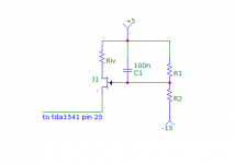
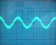
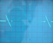
I attached oscillograms of a TDA1541A running in simultaneous mode (pin 27 tied to -5V) with 25% data density and 50Hz DEM, NOS (44.1 KHz, 16 bits). Passive output (150 Ohms I/V with 2K2 bias resistor connected to +5V) amplified by a simple pre-amp.
The output is unfiltered!
It is a worst case air wired setup that can be significantly improved when moving the parts to a decent PCB.
I use plain 78XX and 79XX voltage regulators so nothing special. DEM decoupling caps are 100uF/25V Nichicon UKA. DEM timing cap 1uF WIMA pitch = 2.5mm. Bias resistor between pin 15 and 17: 12K 1%. Plain-A chip. Attenuated digital interface signals (2.4Vpp), 1K series resistors on BCK and data signals to minimise ground-bounce.
Source: iMac running Swinsian (bit-perfect playback verified). Toslink interlink (1.5 meters), DIR9001 receiver (50ps intrinsic jitter), discrete protocol converter that converts 24 bit Left Justified to Simultaneous (same circuit as in my post).
Scope: Philips / Fluke PM3065, setting 2mV/div, probe 1:1.
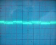
First picture shows a -60dB, 1 KHz test signal.
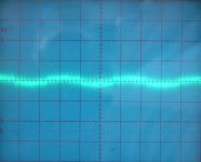
Second picture shows a -70dB, 1 KHz test signal.
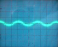
Third picture shows a -80dB, 1 KHz test signal.
Last picture shows -90dB, 1 KHz test signal (96dB is the limit for 16 bits). So the LSB is clearly resolved and remains above the noise floor!
There are tiny spikes visible on all signals, this is the 16 bit data burst followed by a 48 bit silence period of the protocol converter (unavoidable TDA1541A on-chip crosstalk). With I2S we would have continuous noise super imposed on the signal and the trace would appear 3 times wider on the scope because of this switching noise.
When viewing closely you can see slight MSB distortion (remember this is a plain A chip!) that will be inaudible under practical listening conditions.
One can argue about this and that, but these measurements speak for themselves.
I attached oscillograms of a TDA1541A running in simultaneous mode (pin 27 tied to -5V) with 25% data density and 50Hz DEM, NOS (44.1 KHz, 16 bits). Passive output (150 Ohms I/V with 2K2 bias resistor connected to +5V) amplified by a simple pre-amp.
The output is unfiltered!
It is a worst case air wired setup that can be significantly improved when moving the parts to a decent PCB.
I use plain 78XX and 79XX voltage regulators so nothing special. DEM decoupling caps are 100uF/25V Nichicon UKA. DEM timing cap 1uF WIMA pitch = 2.5mm. Bias resistor between pin 15 and 17: 12K 1%. Plain-A chip. Attenuated digital interface signals (2.4Vpp), 1K series resistors on BCK and data signals to minimise ground-bounce.
Source: iMac running Swinsian (bit-perfect playback verified). Toslink interlink (1.5 meters), DIR9001 receiver (50ps intrinsic jitter), discrete protocol converter that converts 24 bit Left Justified to Simultaneous (same circuit as in my post).
Scope: Philips / Fluke PM3065, setting 2mV/div, probe 1:1.
First picture shows a -60dB, 1 KHz test signal.
Second picture shows a -70dB, 1 KHz test signal.
Third picture shows a -80dB, 1 KHz test signal.
Last picture shows -90dB, 1 KHz test signal (96dB is the limit for 16 bits). So the LSB is clearly resolved and remains above the noise floor!
There are tiny spikes visible on all signals, this is the 16 bit data burst followed by a 48 bit silence period of the protocol converter (unavoidable TDA1541A on-chip crosstalk). With I2S we would have continuous noise super imposed on the signal and the trace would appear 3 times wider on the scope because of this switching noise.
When viewing closely you can see slight MSB distortion (remember this is a plain A chip!) that will be inaudible under practical listening conditions.
One can argue about this and that, but these measurements speak for themselves.
Attachments
Hi esgigt,
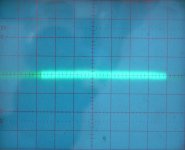
And here are the oscillograms of the DEM clock (1V/div, 5ms/div) and 50Hz DEM ripple on one of the 14 active divider decoupling pins (2mV/div, 5ms/div).
The brightness fluctuations are caused by the low scope scanning frequency and the exposure time of the camera.
The DEM repetition rate is roughly 4 divisions, 4 * 5 = 20ms 1/0.02 = 50Hz.
Decoupling caps, 14 x 100uF/25V Nichicon UKA, plus connected to GND. DEM oscillator timing cap 1uF/50V WIMA r=2.5mm. Bias resistor 12K 1% between pins 15 and 17.
Attachments

- Home
- Source & Line
- Digital Line Level
- Building the ultimate NOS DAC using TDA1541A