OK. I found it (took two minutes) together with an excellent explanation from John abouts its advantages, that I took the liberty to copy...
- Good matching and thermal tracking of both paralleled DAC chips (both DAC sections are located on the same chip).
- Noise / jitter spectrum only relates to one channel that is being processed by that chip instead of a mix from L and R channel.
- Greatly reduced crosstalk between L and R channels. Crosstalk significantly increases when paralleling multiple stereo DAC chips.
- Tolerances in full scale current between L and R channel on the same chip that are related to chip design are cancelled as the same tolerances now occur for both channels.
DAC chips have different propagation delay between BCK / LE signal change and output latching. This time can be measured with a frequency counter.
This means that when paralleling DAC chips that have different propagation delay, the outputs won’t latch exactly simultaneously but rather one after the other. Propagation delay can also change with thermal drift (not constant).
This can introduce significant jitter. Jitter amplitude and spectrum change with amount of paralleled DAC chips and the thermal drift in all DAC chips ensures that sound quality isn’t constant.
Matched DAC sections (located on the same chip) with excellent thermal tracking will minimise this issue with propagation delay (changes). This again can be measured with a frequency counter.
One has to trigger the counter with the BCK / LE signal and stop counting as soon as a new sample is latched at the output. 0dB Square wave test signal can be used for this. The measurement shows tolerances in propagation delay and change of propagation delay as a result of chip temperature changes.
When stacking TDA1543 chips, the chips in the center of the stack get hotter, so propagation delay of these chips will already be quite different from the propagation delay of chips located at the top or bottom of the stack. This, together with tolerances in propagation delay ensures high jitter levels due to non-simultaneous latching.
Similar issues also occur with non-matched delta sigma DAC chips that are not thermally coupled.
So in general it is not a good idea to simply parallel randomly selected unmatched DAC chips as this will almost certainly lead to degraded sound quality compared to a single DAC chip.
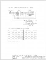
Dual mono configuration can be useful to double full scale output current (better switching characteristics, lower I/V resistor value for same output signal amplitude). Since the full scale current of the TDA1543 for example is rather low (2.3 … 2.5mA) and on-chip crosstalk is rather high, it is a good idea to use these chips in dual mono mode.
Attachments
Yes dear Eldam, I am better than CNC machine tool, hehe. I used a "Dremel". Not ellegant but eficacious.
.
I found it looking very nice, just speaking about looks . It makes me thought to this man : Le site documentaire sur Pierre Soulages : many black to less black light games and clais-obscur with light and bright dark like painters !
Would like having something like your photograph 2 but more hugger for a painter on a wall ! I like it very much !
I'm odd sometimes ! I was not speaking about soldering efficienty and audio result but just about looking !ecdesigns; If you like the result you may have a look at Sowther said:Hi John,
I have implemented the suggested shema and I am happy with it, thanks. Some minor changes, all resistors OHMITE nonmagnetic carbon comp, litycs VISHAY SAL, bypass Pana solid,Russian styrol NOS.
As soon as I can afford it will order better trafos with same or similar ratio.
Regards,
Ignat
Attachments
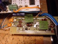
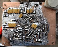
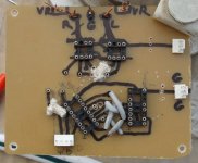
Second DUAL-MONO unit...
without problems this time.
This goes into the SD card player with "variable resistance-transimpedance amplifier" output, but I think now that it is excessive and perhaps I shall go direct out though "variable resistor" and maybe DC coupled with John's idea.
Sounds very powerful, but I miss the Bybee's in the BCK and DATA lines from the previous DAC.
I have still to add the 1uF film caps on the power pins of the DAC chips.
How to select the best 1543 DAC chips without expensive equipment???
Some more art:
Thanks -EC-!
M.
Attachments
Last edited:
How to select the best 1543 DAC chips without expensive equipment???
Hi, I select them for low level linearity by ear! I pick a quiet passage from a purist/acoustic recording and further attenuate it digitally, then listen to that with the analog volume fully open.
Edit: done at night when background noise is lowest! And sitting very close to the speakers.
Last edited:
Hi, I select them for low level linearity by ear! I pick a quiet passage from a purist/acoustic recording and further attenuate it digitally, then listen to that with the analog volume fully open.
Edit: done at night when background noise is lowest! And sitting very close to the speakers.
OK.
Thank you very much.
M.
Hi maxlorenz,
The I2S interface is a necessary evil with all existing DAC (chips). I2S switching noise spectrum crosstalks through the on-chip circuits and changes the DAC chip output spectrum and related sound signature. This impact is rather big and it contributes to the typical digital sound signature.
I2S attenuators and I2S signal bandwidth reduction help a little bit but won’t solve this fundamental issue as the on-chip circuits copy and distribute the I2S switching spectrum.
Late 2014 when I used DAC chips for the last time, I used a different I2S clocking scheme and two DAC chips. This reduced the impact of I2S switching noise by 75%.
Now with Bybees... 
The I2S interface is a necessary evil with all existing DAC (chips). I2S switching noise spectrum crosstalks through the on-chip circuits and changes the DAC chip output spectrum and related sound signature. This impact is rather big and it contributes to the typical digital sound signature.
I2S attenuators and I2S signal bandwidth reduction help a little bit but won’t solve this fundamental issue as the on-chip circuits copy and distribute the I2S switching spectrum.
Late 2014 when I used DAC chips for the last time, I used a different I2S clocking scheme and two DAC chips. This reduced the impact of I2S switching noise by 75%.
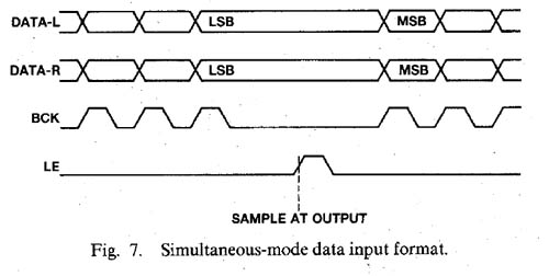
Simultaneous Mode
May I suggest using the TDA1541 in simultaneous mode?
Credits go to Pedja Rogic.
A Philips player with TDA1540 DACs is easy to modify to accomodate the TDA1541 (NON OS)
Jitter does not seem to be an issue as a clock mod did not make any change to the sound.
May I suggest using the TDA1541 in simultaneous mode?
Credits go to Pedja Rogic.
A Philips player with TDA1540 DACs is easy to modify to accomodate the TDA1541 (NON OS)
Jitter does not seem to be an issue as a clock mod did not make any change to the sound.
I have done it on a Marantz CD74, it worked fine. For SAA7210-based machines you need an I2S splitter circuit, since that decoder chip has no simultaneous mode. This is independent of OS or NOS (i.e. the digital filter is installed or removed).May I suggest using the TDA1541 in simultaneous mode?
Credits go to Pedja Rogic.
A Philips player with TDA1540 DACs is easy to modify to accomodate the TDA1541 (NON OS)
Jitter does not seem to be an issue as a clock mod did not make any change to the sound.
Hi maxlorenz,
The I2S interface is a necessary evil with all existing DAC (chips). I2S switching noise spectrum crosstalks through the on-chip circuits and changes the DAC chip output spectrum and related sound signature. This impact is rather big and it contributes to the typical digital sound signature.
I2S attenuators and I2S signal bandwidth reduction help a little bit but won’t solve this fundamental issue as the on-chip circuits copy and distribute the I2S switching spectrum.
Late 2014 when I used DAC chips for the last time, I used a different I2S clocking scheme and two DAC chips. This reduced the impact of I2S switching noise by 75%.
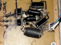
Hello dear -EC-,
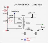
This circuit provides 1,6V for BCK and WS (from SD card player) and 1,2V for DATA. I was tempted to add the attenuators but rejected the idea. Fortunatelly, I remembered that I had one more Bybee slipstream that I managed to resucitate and that was added to the DATA line, so now both DATA lines (RR and LL) are proberly bybeed. As nobody asked what is the sonic effect, I won't talk, since it always starts controversy...I will only comment that the DAC is unlistenable, in the long term, without them
Three questions dear:
1) can we know the different cloking scheme you referred to above?
2) is your ultimate SD card player in its final version???
3) in my first DUAL MONO DAC, the reference voltage for I/V resistor is 4,3V. I hope my calculation is good and it won't clip. Is 4,3V good enough?
Thank you very much.
Yours truly,
M.
Last edited:
Hi maxlorenz,
The I2S interface is a necessary evil with all existing DAC (chips). I2S switching noise spectrum crosstalks through the on-chip circuits and changes the DAC chip output spectrum and related sound signature. This impact is rather big and it contributes to the typical digital sound signature.
I2S attenuators and I2S signal bandwidth reduction help a little bit but won’t solve this fundamental issue as the on-chip circuits copy and distribute the I2S switching spectrum.
Late 2014 when I used DAC chips for the last time, I used a different I2S clocking scheme and two DAC chips. This reduced the impact of I2S switching noise by 75%.
Thanks for sharing your important insight. I wonder if you have worked out where the switching noise is coming from with I2S coding - presumably theres one main component that you eliminated with the different "clocking scheme" leaving one or more other sources?

1) can we know the different cloking scheme you referred to above?
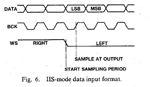
L channel DATA is clocked in R input register of TDA1543 #1.
R channel DATA is clocked in R input register of TDA1543 #2.
So all L & R data is clocked in with 16 clock pulses when WS is “1”. Only the Right channel of each TDA1543 can hold data as DATA can only be clocked in when WS = "1".
Then BCK and DATA signals are shut down completely (total switching silence on the chip). Since I am only feeding clock signals to both TDA1543 chips during 16 of the available 64 pulses I reduce average switching noise levels by 75%.
In order to latch the outputs of both TDA1543 chips I multiplex a LE signal on BCK that produces a single LE transient after WS has gone low.
So the BCK input of both TDA1543 chips acts as both, BCK and LE input. This all is within the permissible specs of I2S.
By reducing on-chip switching noise by 75%, on-chip jitter levels are also reduced.
This requires a suitable I2S to quasi simultaneous mode converter. L & R signal data needs to be lined up too, this requires some shift registers.
OooK. I'll try to digest your "silence mode" DAC arrangement...
I seem to recall the TDA1541 datasheet talked something similar to this...edit: figure n°7 of the presentation paper to the IEEE by H. Schouwenaars at al.
Thanks.
M.
Last edited:
Finally someone else decided to use only the right channel of the chips!
I did it for the audible difference alone. For my 16 chips or so, the right channel is always the better one.
Edit: Easily audible using this "method": http://www.diyaudio.com/forums/digi...e-nos-dac-using-tda1541a-535.html#post4242374
I did it for the audible difference alone. For my 16 chips or so, the right channel is always the better one.
Edit: Easily audible using this "method": http://www.diyaudio.com/forums/digi...e-nos-dac-using-tda1541a-535.html#post4242374
L channel DATA is clocked in R input register of TDA1543 #1.
R channel DATA is clocked in R input register of TDA1543 #2.
So all L & R data is clocked in with 16 clock pulses when WS is “1”. Only the Right channel of each TDA1543 can hold data as DATA can only be clocked in when WS = "1".
Then BCK and DATA signals are shut down completely (total switching silence on the chip). Since I am only feeding clock signals to both TDA1543 chips during 16 of the available 64 pulses I reduce average switching noise levels by 75%.
In order to latch the outputs of both TDA1543 chips I multiplex a LE signal on BCK that produces a single LE transient after WS has gone low.
So the BCK input of both TDA1543 chips acts as both, BCK and LE input. This all is within the permissible specs of I2S.
By reducing on-chip switching noise by 75%, on-chip jitter levels are also reduced.
This requires a suitable I2S to quasi simultaneous mode converter. L & R signal data needs to be lined up too, this requires some shift registers.
Last edited:
...This requires a suitable I2S to quasi simultaneous mode converter. L & R signal data needs to be lined up too, this requires some shift registers.
Is this basically provided by Ian's I2S to PCM board in simultaneous mode?
Was it the SAA7030 which splitted L&R Datas in two channels for the two TDA1540 dac chips ?
I read few time ago the SAA chips can be "less worst" if one provides a clean standalone regulated PS to feed them (not shared with the dac chip(s) )
With any dac chips (even the mono ones like TDA1540 or AD1862, PCM1704, etc) : does the non concistency into the factory production between 2 dac chips in a standalone DAC as said in this thread a long time ago (when 2 TDA1541 circuit were gave up for jitter reasons) be solved by this method or add also a jitter (due to the non concistency inside the dac chips itselves : not solved by any synchron signals before as the jitter is the result of the dispersions characteristics of the dac chips itselves and not the signal injected before ?)
Shift register chip : cause of jitter or "switching spectrum noise jitter" itself ?
John,
Is there a level of Jitter measured by the instruments which can not be hearable anymore (for the trebles like for the bass in relation to the scope "form" of the square signal when measuring the jitter) ? I remember also than the clock dem sync with the tda1541was giving up as well : the clock divider on the clock circuit were a cause of jitter iirc ! Not the same or a sort of "same" when mutiplexing again the LE on BCLK channel ? Sorry if I'm not understamble enough... I have diffcilties to follow the process you have been describing just above !
(Though if Pedja Rogic uses L&R splitted signals, he uses also the DEM sync feeding with an external clock instead the dem sync cap of few pico).
I keep in mind you choosed finally 100 pico silver mica in smd here with the ingenious 6k8 resistors. Does finally in the actual state of your research two tda1543 with an active clock scheme I2S reworked as you do, give a better result than a standalone TDA1541 (e.g. with simultaneous mode) with the simple dem sync cap (passive) ?
I don't know for the TDA1543 but imho the TDA1545A has the best trebles vs a TDA1541 (though the TDA1541 is better in the rest of the whole register : below the trebles ).
John, did you finally experiment the TDA1387 like T. Loesch did : don't remember if we alwats talked about it in this long thread ?
regards
I read few time ago the SAA chips can be "less worst" if one provides a clean standalone regulated PS to feed them (not shared with the dac chip(s) )
With any dac chips (even the mono ones like TDA1540 or AD1862, PCM1704, etc) : does the non concistency into the factory production between 2 dac chips in a standalone DAC as said in this thread a long time ago (when 2 TDA1541 circuit were gave up for jitter reasons) be solved by this method or add also a jitter (due to the non concistency inside the dac chips itselves : not solved by any synchron signals before as the jitter is the result of the dispersions characteristics of the dac chips itselves and not the signal injected before ?)
Shift register chip : cause of jitter or "switching spectrum noise jitter" itself ?
John,
Is there a level of Jitter measured by the instruments which can not be hearable anymore (for the trebles like for the bass in relation to the scope "form" of the square signal when measuring the jitter) ? I remember also than the clock dem sync with the tda1541was giving up as well : the clock divider on the clock circuit were a cause of jitter iirc ! Not the same or a sort of "same" when mutiplexing again the LE on BCLK channel ? Sorry if I'm not understamble enough... I have diffcilties to follow the process you have been describing just above !
(Though if Pedja Rogic uses L&R splitted signals, he uses also the DEM sync feeding with an external clock instead the dem sync cap of few pico).
I keep in mind you choosed finally 100 pico silver mica in smd here with the ingenious 6k8 resistors
. Does finally in the actual state of your research two tda1543 with an active clock scheme I2S reworked as you do, give a better result than a standalone TDA1541 (e.g. with simultaneous mode) with the simple dem sync cap (passive) ?I don't know for the TDA1543 but imho the TDA1545A has the best trebles vs a TDA1541 (though the TDA1541 is better in the rest of the whole register : below the trebles ).
John, did you finally experiment the TDA1387 like T. Loesch did : don't remember if we alwats talked about it in this long thread ?
regards
Last edited:
Hi Kazap,
Every time one of the I2S signals changes state it produces a switching spike (ground-bounce). The effect can be easily demonstrated by shutting down all I2S signals halfway the sample period. One would see a noisy DAC output signal when I2S is active and a flat line when I2S is shut down. This is a rather alarming problem that prevents transparent sound reproduction.
Apart from the switching noise, a jitter spectrum is introduced that relates to the I2S signals. The I2S DATA signal is most problematic as it introduces deterministic (data related) jitter spectrum on the output of the DAC chip.
Possible workaround is minimising the amount of I2S signal transients.
Similar, the TDA1540, TDA1541, and TDA1541A have an on-chip DEM circuit that adds more switching noise (ground-bounce). The DEM oscillator frequency / phase is modulated by the data and output signal and also introduces deterministic jitter.
Thanks for sharing your important insight. I wonder if you have worked out where the switching noise is coming from with I2S coding
Every time one of the I2S signals changes state it produces a switching spike (ground-bounce). The effect can be easily demonstrated by shutting down all I2S signals halfway the sample period. One would see a noisy DAC output signal when I2S is active and a flat line when I2S is shut down. This is a rather alarming problem that prevents transparent sound reproduction.
Apart from the switching noise, a jitter spectrum is introduced that relates to the I2S signals. The I2S DATA signal is most problematic as it introduces deterministic (data related) jitter spectrum on the output of the DAC chip.
Possible workaround is minimising the amount of I2S signal transients.
Similar, the TDA1540, TDA1541, and TDA1541A have an on-chip DEM circuit that adds more switching noise (ground-bounce). The DEM oscillator frequency / phase is modulated by the data and output signal and also introduces deterministic jitter.
- Home
- Source & Line
- Digital Line Level
- Building the ultimate NOS DAC using TDA1541A