Hi studiostevus,
The signal on the DEM oscillator shows that the DEM oscillator isn't functioning like it should. One should measure a clean sawtooth-shaped signal.
I attached an oscillogram of the DEM clock synced with 2.8224 MHz measured on the MK11 DAC.
Next oscillogram shows DEM clock synced with 352.8 KHz from an earlier design. The spikes on the active divider output signal (filter cap removed) are caused by on-chip crosstalk with BCK.
Easy way to check if the oscillator is actually providing clock pulses to the shift registers and bit switches is removing one of the (100nF) filter caps and checking for step-shaped signal using sensitivity of 20mV / div.
Synchronizing a DEM oscillator with external clock signals isn't easy. The synchronizing circuit must be carefully matched with DEM oscillator properties.
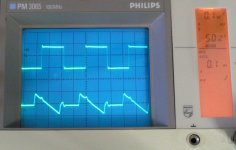
Well have a look here....
Upper trace: pin16 (dem)
Lower trace: pin bck
Doesnt look good.... Does it?
The signal on the DEM oscillator shows that the DEM oscillator isn't functioning like it should. One should measure a clean sawtooth-shaped signal.
I attached an oscillogram of the DEM clock synced with 2.8224 MHz measured on the MK11 DAC.
Next oscillogram shows DEM clock synced with 352.8 KHz from an earlier design. The spikes on the active divider output signal (filter cap removed) are caused by on-chip crosstalk with BCK.
Easy way to check if the oscillator is actually providing clock pulses to the shift registers and bit switches is removing one of the (100nF) filter caps and checking for step-shaped signal using sensitivity of 20mV / div.
Synchronizing a DEM oscillator with external clock signals isn't easy. The synchronizing circuit must be carefully matched with DEM oscillator properties.
Attachments
power supply question
John
how do you compare your last discrete shunt regulator posted http://www.diyaudio.com/forums/digi...e-nos-dac-using-tda1541a-431.html#post2997059 with led referenced regulator posted http://www.diyaudio.com/forums/digi...e-nos-dac-using-tda1541a-297.html#post1884018 either measure bandwidth and impedance and perceived sound
Hi samoloko,
Shunt regulator has advantage that C-E or S-D stray capacitance is in parallel with the connected load and thus helps to decouple the output voltage.
In series regulators the C-E or S-D stray capacitance helps to feed unwanted noise into the connected load.
CCS also puts C-E or S-D stray capacitance between noisy transformer secondary and shunt regulator. That's why I now use capacitance multiplier circuits for ripple rejection (these still pass RF noise through C-E stray capacitance) followed by a balanced RC filter that offers low pass filtering and current limiting for the shunt regulator.
how do you compare your last discrete shunt regulator posted Building the ultimate NOS DAC using TDA1541A with led referenced regulator posted Building the ultimate NOS DAC using TDA1541A either measure bandwidth and impedance and perceived sound
Shunt regulator has advantage that C-E or S-D stray capacitance is in parallel with the connected load and thus helps to decouple the output voltage.
In series regulators the C-E or S-D stray capacitance helps to feed unwanted noise into the connected load.
CCS also puts C-E or S-D stray capacitance between noisy transformer secondary and shunt regulator. That's why I now use capacitance multiplier circuits for ripple rejection (these still pass RF noise through C-E stray capacitance) followed by a balanced RC filter that offers low pass filtering and current limiting for the shunt regulator.
Hi JOSI1,
Like I mentioned in previous post, DEM clock can be synchronized with either BCK or WS.
In previous designs I triggered or synchronized the DEM clock with BCK.
This has some disadvantages as s3tup pointed out in post #4405.
Electronic switches in active divider cause switching spikes on the averaged output signal. These spikes have specific pulse width. The higher the DEM clock rate the more these switching spikes will dominate the active divider output signal shape.
Cleanest sample steady current could be obtained by synchronizing the DEM clock with WS, then we would add only 2 fixed switching spikes to the already present 128 spikes from BCK (130 switching spikes in total). This means that one DEM cycle (4 switch changes) is completed after every 4 samples.
Other advantage is that the filter caps and filter circuit become less critical as DEM clock rate is now reduced to 44.1 KHz (NOS).
Based on filter cap value of 100nF @ 200,000 Hz, DEM clock rate of 44,100 Hz would require 470nF filter caps (closest value). Since I already had 1uF filter caps installed I could easily test 44.1 KHz DEM clock with minimum changes to the existing circuit.
The DEM circuit ensures that the 6 MSBs plus the input current for the 10 bit passive current divider always remain very closely matched, despite on-chip tolerances / chip aging. Keep in mind that even slightest errors in MSBs also lead to errors in the LSB range. So all bits contribute to the final bit accuracy.
The DEM oscillator now oscillates on the timing capacitor again, so 2K2 resistors need to be removed. For synchronization with WS, 33pF timing cap value is no longer valid.
In short, i conclude the following:
1. Fdem should be as low as possible, but at least f_ws.
2. Although you call it synchronized, it essentially is a free running oscillator with frequency close to ws.
3. Cosc should be quite high to achieve such frequency (470nf Cosc gives 176khz, no?)
3. The filter caps should at least be 470nf in order to provide adequate filtering to allow such low dem frequency.
Just trying to distill the learnings for myself here....
I just tried free running DEM oscillator using a 10nf cap, which results in approx 120khz.
Some observations:
- digital artifacts on low level signals have disappeared, sound is good again
- measuring at pin 16 gives the normal oscillator picture, so it is working
- i had a good look with the scope on pin 16 whether there were any peaks visible on the dem osc signal on the transients of bck... There were not, there is no visible crosstalk, even using this non-synchronized frequency (120khz)
In short, i conclude the following:
1. Fdem should be as low as possible, but at least f_ws.
2. Although you call it synchronized, it essentially is a free running oscillator with frequency close to ws.
3. Cosc should be quite high to achieve such frequency (470nf Cosc gives 176khz, no?)
3. The filter caps should at least be 470nf in order to provide adequate filtering to allow such low dem frequency.
Just trying to distill the learnings for myself here....
really 470 nF (thousand times as much as the spec sheet)?
really 470 nF (thousand times as much as the spec sheet)?
pF
So, the issue was in running the DEM with too high rate?
Seems like it yes. I am using a 1998 chip, but 33pf (3mhz?) seems to be too much, even in what i believe to be a good layout.
I am wondering though where to take the dem frequency, considering that i didnt find any evidence of crosstalk (which was the prime reason of choosing a dem frequency equal to either bck or ws or a multiple of these)... Does it not matter what frequency is chosen after all?
Hi studiostevus,
DEM oscillator produces pulses (rising and falling edge of clock signal) that crosstalk to other on-chip circuits and also appear on the DAC output. These are the 40mVpp spikes that are visible on oscillogram in post #4421 showing the step signal measured on one of the 14 -unfiltered- active divider outputs.
The higher the DEM oscillator rate with respect to WS, the more "spikes" appear on other on-chip circuits, the more interference through crosstalk is generated.
With higher DEM oscillator rates, the impact of given switching pulse width and finite switching time will distort the signal shape at the active divider outputs. The switching spikes are relatively large compared to total switch closed time and the current needs some time to settle after switching, so the flat current steps now turn into a curved signal as the bit current has too little time to settle between switch changes.
When DEM oscillator frequency drops below 20 KHz there is the risk of audible crosstalk in the audio band as DEM oscillator now runs on a frequency that falls within the audio band.
Free running DEM clock can result in DEM oscillator transients coinciding with the latch trigger signal. This in turn can change the exact moment of latching (crosstalk) and thus increase unwanted on-chip jitter.
The TDA1541A output latch is triggered (exact moment the output sample value changes) on the first positive going edge of BCK -after- WS has gone from "1" to "0".
After it's synchronized with WS or BCK, the DEM oscillator is locked to these signals and is therefore no longer free running.
470pF gives around 200 KHz. I used 33pF for 2.8224 MHz.
10nF (0.01uF, 10,000pF) gives around 8 … 9 KHz. This requires filter cap value of around 2.2uF for each of the 14 active divider outputs.
The crosstalk (peaks) I mentioned were measured on the one of the 14 active divider outputs with -filter cap removed-. The amplitude is around 40mVpp. Peaks cannot be measured on pin 16 / 17 as the peaks are caused by the DEM oscillator itself.
All TDA1541A chips have to meet similar specs (max. frequency) so all TDA1541A chip DEM oscillators should run perfectly on 2.8224 Mhz as this is well within max. frequency of around 7 MHz.
1. Fdem should be as low as possible, but at least f_ws.
DEM oscillator produces pulses (rising and falling edge of clock signal) that crosstalk to other on-chip circuits and also appear on the DAC output. These are the 40mVpp spikes that are visible on oscillogram in post #4421 showing the step signal measured on one of the 14 -unfiltered- active divider outputs.
The higher the DEM oscillator rate with respect to WS, the more "spikes" appear on other on-chip circuits, the more interference through crosstalk is generated.
With higher DEM oscillator rates, the impact of given switching pulse width and finite switching time will distort the signal shape at the active divider outputs. The switching spikes are relatively large compared to total switch closed time and the current needs some time to settle after switching, so the flat current steps now turn into a curved signal as the bit current has too little time to settle between switch changes.
When DEM oscillator frequency drops below 20 KHz there is the risk of audible crosstalk in the audio band as DEM oscillator now runs on a frequency that falls within the audio band.
Free running DEM clock can result in DEM oscillator transients coinciding with the latch trigger signal. This in turn can change the exact moment of latching (crosstalk) and thus increase unwanted on-chip jitter.
The TDA1541A output latch is triggered (exact moment the output sample value changes) on the first positive going edge of BCK -after- WS has gone from "1" to "0".
2. Although you call it synchronized, it essentially is a free running oscillator with frequency close to ws.
After it's synchronized with WS or BCK, the DEM oscillator is locked to these signals and is therefore no longer free running.
3. Cosc should be quite high to achieve such frequency (470nf Cosc gives 176khz, no?)
470pF gives around 200 KHz. I used 33pF for 2.8224 MHz.
I just tried free running DEM oscillator using a 10nf cap, which results in approx 120khz.
10nF (0.01uF, 10,000pF) gives around 8 … 9 KHz. This requires filter cap value of around 2.2uF for each of the 14 active divider outputs.
- i had a good look with the scope on pin 16 whether there were any peaks visible on the dem osc signal on the transients of bck... There were not, there is no visible crosstalk, even using this non-synchronized frequency (120khz)
The crosstalk (peaks) I mentioned were measured on the one of the 14 active divider outputs with -filter cap removed-. The amplitude is around 40mVpp. Peaks cannot be measured on pin 16 / 17 as the peaks are caused by the DEM oscillator itself.
Seems like it yes. I am using a 1998 chip, but 33pf (3mhz?) seems to be too much, even in what i believe to be a good layout.
All TDA1541A chips have to meet similar specs (max. frequency) so all TDA1541A chip DEM oscillators should run perfectly on 2.8224 Mhz as this is well within max. frequency of around 7 MHz.
Hi John,
In this context, what do you mean with 'synchronized' and 'locked' ?
Regarding synchronization: Reading from one of your post some days ago, it seemed that you concluded that it was impossible/difficult to trigger DEM oscillator with WS/BCK due to prop. delays of the internal and external circuitry. This causes the spikes you showed on post 4421 on the DEM signal.
Hence, I concluded you meant with synchronization free running DEM clock (using a cap between pin 16 and 17) which achieves the same frequency as WS or BCK (e.g. 33pf for 2.8MHz BCK).
If that is the case, please help me understand the 'locking' concept you talk about. From the internal TDA circuitry, I couldn't see how this 'locking' would be done...
So... as low as possible, minumum F_ws...Hi studiostevus,
DEM oscillator produces pulses (rising and falling edge of clock signal) that crosstalk to other on-chip circuits and also appear on the DAC output. These are the 40mVpp spikes that are visible on oscillogram in post #4421 showing the step signal measured on one of the 14 -unfiltered- active divider outputs.
The higher the DEM oscillator rate with respect to WS, the more "spikes" appear on other on-chip circuits, the more interference through crosstalk is generated.
With higher DEM oscillator rates, the impact of given switching pulse width and finite switching time will distort the signal shape at the active divider outputs. The switching spikes are relatively large compared to total switch closed time and the current needs some time to settle after switching, so the flat current steps now turn into a curved signal as the bit current has too little time to settle between switch changes.
When DEM oscillator frequency drops below 20 KHz there is the risk of audible crosstalk in the audio band as DEM oscillator now runs on a frequency that falls within the audio band.
After it's synchronized with WS or BCK, the DEM oscillator is locked to these signals and is therefore no longer free running.
In this context, what do you mean with 'synchronized' and 'locked' ?
Regarding synchronization: Reading from one of your post some days ago, it seemed that you concluded that it was impossible/difficult to trigger DEM oscillator with WS/BCK due to prop. delays of the internal and external circuitry. This causes the spikes you showed on post 4421 on the DEM signal.
Hence, I concluded you meant with synchronization free running DEM clock (using a cap between pin 16 and 17) which achieves the same frequency as WS or BCK (e.g. 33pf for 2.8MHz BCK).
If that is the case, please help me understand the 'locking' concept you talk about. From the internal TDA circuitry, I couldn't see how this 'locking' would be done...
You are right, I misread the frequency10nF (0.01uF, 10,000pF) gives around 8 … 9 KHz. This requires filter cap value of around 2.2uF for each of the 14 active divider outputs.
I see, I was looking for effects of BCK on the DEM Oscillator signal, while the crosstalk you talk about is the other way around (DEM Oscillator affects BCK/WS)The crosstalk (peaks) I mentioned were measured on the one of the 14 active divider outputs with -filter cap removed-. The amplitude is around 40mVpp. Peaks cannot be measured on pin 16 / 17 as the peaks are caused by the DEM oscillator itself.
Interesting... that's what I thought, but could't get it to work...All TDA1541A chips have to meet similar specs (max. frequency) so all TDA1541A chip DEM oscillators should run perfectly on 2.8224 Mhz as this is well within max. frequency of around 7 MHz.
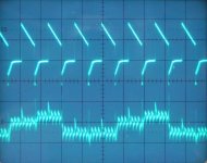
Did another attempt with 33pf 'free running'. This is the picture on my 50mhz scope....
Top is bck @ 2.8mhz
Bottom is dem osc (33pf)
Still doesnt look like a normal multivibrator...
Top is bck @ 2.8mhz
Bottom is dem osc (33pf)
An externally hosted image should be here but it was not working when we last tested it.
Still doesnt look like a normal multivibrator...
44.1 kHz too low ?
The Philips application notes say that the DEM frequency is divided by a factor 4 internally, resulting in a very small ripple at the output with a frequency of (DEM freq)/4 Hz, which may never be within the audio pass band.
This implies a minimum of 80 kHz for the DEM frequency. So it is OK to sync with WS in 4xOS mode where WS = 176.4 kHz (as in the Grundig CD9009), but not in NOS mode where WS = 44.1 kHz because of the little ripple at 11025 Hz. In NOS mode, the 176.4 kHz can be obtained by dividing BCK with flip-flops.
Philips recommend a maximum of 300 kHz for DEM frequency when using the external cap only, because distortion increases due to poorer duty cycle accuracy of the free-running multivibrator above 300 kHz.
I believe that the 300 kHz limit does not apply when the multivibrator is disabled if the DEM shift register duty cycle resulting from the external control circuit is accurate.
Hi grundigger,
Quote from IEEE Journal of solid-state circuits, vol. SC-14, no. 3, June 1979 page 553
"The figure shows that the currents with value I have a ripple with the same frequency as the clock generator f."
Currents with value 2I (two active divider outputs in parallel) should have ripple frequency of f/2. But after measuring all 14 active divider output ripple currents on a number of different TDA1541A chips it turned out this is incorrect. All active divider outputs (including those connected in parallel) show 4-step pattern with ripple frequency of fDEM.
So with 44.1 KHz DEM frequency the ripple current frequency on the active divider output equals 44.1 KHz and this is outside the audio band.
The problem with increasing DEM frequency is that stray capacitances and settling time will have increasing impact (distortion).
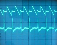
I attached an oscillogram of a DEM clock running at 2.8224 Mhz. The upper trace shows the DEM oscillator output (33pF synced with BCK). The lower trace shows the signal on one active divider output (filter cap removed). The switching pulse takes up around 40% of the total "switch closed" time and will now have significant impact on the value of the averaged active divider output current.
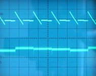
The second oscillogram shows DEM clock running at 44.1 KHz. The upper trace shows the DEM oscillator output (1.82nF synced with WS). The lower trace shows the signal on one active divider output (filter cap removed). The switching pulse is barely visible and only takes up a very small fraction of the total "switch closed" time and will now have very little impact on the value of the averaged active divider output current.
Similar happens with the TDA1541A output signal. The higher the sample rate, the larger the impact of stray capacitance and settling time on the sample.
The Philips application notes say that the DEM frequency is divided by a factor 4 internally, resulting in a very small ripple at the output with a frequency of (DEM freq)/4 Hz, which may never be within the audio pass band.
Quote from IEEE Journal of solid-state circuits, vol. SC-14, no. 3, June 1979 page 553
"The figure shows that the currents with value I have a ripple with the same frequency as the clock generator f."
Currents with value 2I (two active divider outputs in parallel) should have ripple frequency of f/2. But after measuring all 14 active divider output ripple currents on a number of different TDA1541A chips it turned out this is incorrect. All active divider outputs (including those connected in parallel) show 4-step pattern with ripple frequency of fDEM.
So with 44.1 KHz DEM frequency the ripple current frequency on the active divider output equals 44.1 KHz and this is outside the audio band.
Philips recommend a maximum of 300 kHz for DEM frequency when using the external cap only, because distortion increases due to poorer duty cycle accuracy of the free-running multivibrator above 300 kHz.
The problem with increasing DEM frequency is that stray capacitances and settling time will have increasing impact (distortion).
I attached an oscillogram of a DEM clock running at 2.8224 Mhz. The upper trace shows the DEM oscillator output (33pF synced with BCK). The lower trace shows the signal on one active divider output (filter cap removed). The switching pulse takes up around 40% of the total "switch closed" time and will now have significant impact on the value of the averaged active divider output current.
The second oscillogram shows DEM clock running at 44.1 KHz. The upper trace shows the DEM oscillator output (1.82nF synced with WS). The lower trace shows the signal on one active divider output (filter cap removed). The switching pulse is barely visible and only takes up a very small fraction of the total "switch closed" time and will now have very little impact on the value of the averaged active divider output current.
Similar happens with the TDA1541A output signal. The higher the sample rate, the larger the impact of stray capacitance and settling time on the sample.
Attachments
Hi all, are the following still being used as best examples:
1. Charge transfer power supply?
2. 3 diode rectifier? (How does this relate to the charge transfer ps?)
3. The LED voltage regulators?
I am buidling a 1543 dac and would like to use the best ideas for power supplies.
Many thanks
Ryan
1. Charge transfer power supply?
2. 3 diode rectifier? (How does this relate to the charge transfer ps?)
3. The LED voltage regulators?
I am buidling a 1543 dac and would like to use the best ideas for power supplies.
Many thanks
Ryan
Hi Dr.H,
1. Charge transfer power supply is no longer used because RF passes transistors / FETs through C-E / S-D.
2. The 3 diode rectifier can still be used as it reduces switching noise and only adds 0.4 … 0.6 V drop / diode.
3. I now use shunt voltage regulators with filtered LED reference.
The latest power supplies are constructed as follows:
Isolated transformer winding > RF filter > rectifier > smoothing cap > capacitance multiplier in plus lead > capacitance multiplier in minus lead > 6th order balanced RC filter / current limiter > discrete shunt regulator > local SMD film / NPO decoupling caps.
The isolated winding enables "floating" supplies that can be easily fed into a star ground without one supply polluting the other through common ground leads.
The RF filters attenuate mains RF noise (that passes transformer stray capacitance).
The rectifiers and smoothing caps produce a DC voltage with certain ripple voltage.
The capacitance multiplier in the plus lead attenuates ripple by approx. 2000 times.
The capacitance multiplier in the minus lead attenuates remaining ripple by approx. 2000 times.
The 6th order balanced RC filter attenuates ripple / noise by another 36dB.
Typical input ripple voltage equals 300mVpp. After the first capacitance multiplier this is reduced to 150uVpp. After the second capacitance multiplier it is further reduced to 75nVpp. After the balanced 6th order RC filter it is reduced to little over 1nVpp.
The shunt regulator theoretically reduces remaining noise by up to factor 160,000 (down to 6.25 Femto volts). In practice the noise level is limited by component noise, reference voltage properties and EMI. However, mains noise / ripple is reduced to vanishing low levels and is basically eliminated.
Local decoupling caps are required as shunt regulator bandwidth is limited. I am now using a combination of SMD PPS film caps and 220nF ceramic NPO caps. I am no longer using X7R / Y5V decoupling caps due to piezoelectric effects, distortion, poor stability, and poor mechanical strength.
Hi all, are the following still being used as best examples:
1. Charge transfer power supply?
2. 3 diode rectifier? (How does this relate to the charge transfer ps?)
3. The LED voltage regulators?
I am buidling a 1543 dac and would like to use the best ideas for power supplies.
Many thanks
Ryan
1. Charge transfer power supply is no longer used because RF passes transistors / FETs through C-E / S-D.
2. The 3 diode rectifier can still be used as it reduces switching noise and only adds 0.4 … 0.6 V drop / diode.
3. I now use shunt voltage regulators with filtered LED reference.
The latest power supplies are constructed as follows:
Isolated transformer winding > RF filter > rectifier > smoothing cap > capacitance multiplier in plus lead > capacitance multiplier in minus lead > 6th order balanced RC filter / current limiter > discrete shunt regulator > local SMD film / NPO decoupling caps.
The isolated winding enables "floating" supplies that can be easily fed into a star ground without one supply polluting the other through common ground leads.
The RF filters attenuate mains RF noise (that passes transformer stray capacitance).
The rectifiers and smoothing caps produce a DC voltage with certain ripple voltage.
The capacitance multiplier in the plus lead attenuates ripple by approx. 2000 times.
The capacitance multiplier in the minus lead attenuates remaining ripple by approx. 2000 times.
The 6th order balanced RC filter attenuates ripple / noise by another 36dB.
Typical input ripple voltage equals 300mVpp. After the first capacitance multiplier this is reduced to 150uVpp. After the second capacitance multiplier it is further reduced to 75nVpp. After the balanced 6th order RC filter it is reduced to little over 1nVpp.
The shunt regulator theoretically reduces remaining noise by up to factor 160,000 (down to 6.25 Femto volts). In practice the noise level is limited by component noise, reference voltage properties and EMI. However, mains noise / ripple is reduced to vanishing low levels and is basically eliminated.
Local decoupling caps are required as shunt regulator bandwidth is limited. I am now using a combination of SMD PPS film caps and 220nF ceramic NPO caps. I am no longer using X7R / Y5V decoupling caps due to piezoelectric effects, distortion, poor stability, and poor mechanical strength.
DEM again
Hello -ecdesigns-
Thanks for your reply in post 4434. Perhaps both you and Philips are correct. The DEM network has 4 states and full cycles occur with a frequency of fDEM/4. The ripple at the DAC output is a function of the ripples of all active divider stages, which have various amplitudes. With differing phase, do they combine to produce the very small fDEM/4 ripple component at the output which Philips claim exists ?
To quote Philips:
"In the basic application where an external capacitor is used, the oscillator frequency is about 200kHz. The higher this frequency the lower the filter capacitor values you need at pins 7-13 and 24-18 for the same DEM frequency but also the lower the duty cycle accuracy of the DEM frequency (See [4]). The DEM frequency is divided by a factor 4 internally, resulting in a very small ripple at the output with a frequency of (DEM freq)/4 Hz. This frequency may never be within the audio pass band. So, there is a maximum as well as a minimum DEM frequency. A DEM frequency up to 300kHz is allowed but at higher frequencies there is some increase of distortion mainly at the low signal frequencies. Figure 18 shows the relative deterioration of the (D+N)/S at different frequencies as a function of the DEM frequency with respect to (D+N)/S at a DEM frequency of 150 kHz."
The June 1986 IEEE paper about the TDA1541 states "The interchanging network consists of Darlington differential pairs which are optimised for base current losses and interchanging frequency". The original design parameter for the interchanging frequency (i.e. DEM frequency) is 250 kHz. Darlingtons are also used to isolate the current switching from the filtering. Might their speed limit determine the maximum effective DEM frequency?
Philips give an 'Alternative External Control Circuit' as used in the Grundig CD9009, and suggest 176.4 kHz. I believe that 176.4 kHz is a good choice of DEM frequency in both NOS and OS mode, because it gives the correct output current for each CD sample with the minimum DEM switching energy. Even in 4/8xOS mode at a 176.4 kHz or 352.8 kHz sample rate, it still works well because the interpolated samples add no information about the wave, so the average DAC output current during each original CD sample period is correct, despite each oversample using only one DEM state. However, it is desirable to use all four DEM states for each CD sample to get an accurate current at the output to correctly recreate the wave. In NOS mode, WS at 44.1 kHz is too slow and BCK is too fast, so BCK can be divided by flip-flops to get 176.4 kHz (or 352.8 kHz) to synchronise the DEM using the Philips/Grundig or some other control circuit.
Hello -ecdesigns-
To quote Philips:
"In the basic application where an external capacitor is used, the oscillator frequency is about 200kHz. The higher this frequency the lower the filter capacitor values you need at pins 7-13 and 24-18 for the same DEM frequency but also the lower the duty cycle accuracy of the DEM frequency (See [4]). The DEM frequency is divided by a factor 4 internally, resulting in a very small ripple at the output with a frequency of (DEM freq)/4 Hz. This frequency may never be within the audio pass band. So, there is a maximum as well as a minimum DEM frequency. A DEM frequency up to 300kHz is allowed but at higher frequencies there is some increase of distortion mainly at the low signal frequencies. Figure 18 shows the relative deterioration of the (D+N)/S at different frequencies as a function of the DEM frequency with respect to (D+N)/S at a DEM frequency of 150 kHz."
How important is jitter in the DEM signal anyway?
I am now injecting a derivative of my (not reclocked) WS signal into the DEM oscillator, and confirmed it is locked (visible 4-step signal on the decoupling pins). I am using an smd schottky diode and some resistors between pin1 and pin16.
1. Of course, with DEM be synchronized to WS, some of the problems with crosstalk outlined by John are mitigated, regardless of whether the WS signal is jittery or not (point being is that they are synchronous).
2. A not-reclocked WS signal should be ok as input signal as BCK (which is reclocked in my case) provides the timing for the latching.
However, now that WS becomes the driver for the DEM oscillator as well, what is the impact of any jitter on the WS (= DEM Oscillator) signal?
btw, sounds pretty darn good, much softer/smoother in the mids and highs, and bass has tightened up as well.
Last edited:
- Home
- Source & Line
- Digital Line Level
- Building the ultimate NOS DAC using TDA1541A