Hi AndrewGM,
One could use a 220pF 2 ... 10% film cap in parallel with a 47pF film trimmer. This way the trimmer can be adjusted until the DEM clock locks on an exact multiple of the bit clock, this can be verified with a frequency counter or oscilloscope. The free running DEM clock can still lock to the bit clock because of on-chip crosstalk between both clock signals.
Also, is silver mica ok for the DEM cap in 2% tolerance ? You mentioned 1 % but they are hard to come by.
One could use a 220pF 2 ... 10% film cap in parallel with a 47pF film trimmer. This way the trimmer can be adjusted until the DEM clock locks on an exact multiple of the bit clock, this can be verified with a frequency counter or oscilloscope. The free running DEM clock can still lock to the bit clock because of on-chip crosstalk between both clock signals.
Hi studiostevus,
My aim was ultimate sound quality, and computer-based digital audio sources with USB / Toslink interface failed to provide it.
The best computer-based solution so far is using a highly modified squeezebox player that is slaved by the local masterclock in the DAC. Both SB player and DAC need to be integrated in order to keep I2S interface and masterclock wiring as short as possible.
More chips produce more interference and introduce more clock loads that could degrade masterclock performance. I already tried a dual double-crown version of the MK7 DAC but it failed to provide single chip MK7 performance.
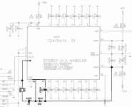
TDA1541A channel matching is not perfect, when implementing a balanced setup, both positive and negative signal half amplitude will differ slightly. This creates a linearity error. Suppose left channel full scale current equals 3.98mA and right channel (also used for left) equals 4.00mA, then there will be a 0.02mA mismatch or almost 8 bits linearity error (based on 61nA LSB current).
More DAC chips also produce more interference and introduce more clock loads. It is likely that a higher clock load on masterclock or divider will also increase propagation delay (capacitive loading increases). This in turn can result in higher jitter levels.
The SD-player with MK7 DAC and latest (prototype) power supply gives the impression of listening to analogue playback equipment. What I was missing in previous designs is highly relaxing super detailed sound on a pitch black background. This was achieved by systematically reducing jitter and interference levels as illustrated on this thread.
The 'compatibility reasons with modern dacs' refers to the SD-transport that was modified to output 64 bits / frame so it could be connected to most modern DAC chips. This also resulted in 2.8224 MHz DEM clock rate in the MK7.
1. What happened to your shift register / one-shot solution for reclocking USB? I read it disappeared since it still generated too much jitter compared to an integrated SD-card solution, but would it still be your preferred solution for working with USB? I am planning to use a mac mini as transport, for simple reasons of GUI and flexibility and looking for the best sounding solution given this transport.
My aim was ultimate sound quality, and computer-based digital audio sources with USB / Toslink interface failed to provide it.
The best computer-based solution so far is using a highly modified squeezebox player that is slaved by the local masterclock in the DAC. Both SB player and DAC need to be integrated in order to keep I2S interface and masterclock wiring as short as possible.
2. You have created many inventive solutions that would be applicable to your earlier models as well (DI8 and DI4). What would happen if you implement the latest DEM, DJA, discrete shunt regs, simplistic output stae, honeycomb resistors, masterclocking, etc. to those models?
More chips produce more interference and introduce more clock loads that could degrade masterclock performance. I already tried a dual double-crown version of the MK7 DAC but it failed to provide single chip MK7 performance.
3. What is your view on balanced setup with 2 dacs? (R+/R- on one chip, L+/L- on the other) ?
TDA1541A channel matching is not perfect, when implementing a balanced setup, both positive and negative signal half amplitude will differ slightly. This creates a linearity error. Suppose left channel full scale current equals 3.98mA and right channel (also used for left) equals 4.00mA, then there will be a 0.02mA mismatch or almost 8 bits linearity error (based on 61nA LSB current).
More DAC chips also produce more interference and introduce more clock loads. It is likely that a higher clock load on masterclock or divider will also increase propagation delay (capacitive loading increases). This in turn can result in higher jitter levels.
4. I read somewhere that mk6 or mk7 would be your last model based on one tda1541. Later I read that you implemented a certain circuit for 'compatibility reasons with modern dacs'. What does the future have in store for us?
The SD-player with MK7 DAC and latest (prototype) power supply gives the impression of listening to analogue playback equipment. What I was missing in previous designs is highly relaxing super detailed sound on a pitch black background. This was achieved by systematically reducing jitter and interference levels as illustrated on this thread.
The 'compatibility reasons with modern dacs' refers to the SD-transport that was modified to output 64 bits / frame so it could be connected to most modern DAC chips. This also resulted in 2.8224 MHz DEM clock rate in the MK7.
John,
Are these FCN6040E105K-S Cornell Dubilier SMD Film Capacitors
the decoupling caps you use? Are you not worried about the high tolerance (10%) ?
Are these FCN6040E105K-S Cornell Dubilier SMD Film Capacitors
the decoupling caps you use? Are you not worried about the high tolerance (10%) ?
Hi studiostevus,
TDA1541A channel matching is not perfect, when implementing a balanced setup, both positive and negative signal half amplitude will differ slightly. This creates a linearity error. Suppose left channel full scale current equals 3.98mA and right channel (also used for left) equals 4.00mA, then there will be a 0.02mA mismatch or almost 8 bits linearity error (based on 61nA LSB current).
And?
Why would that be a problem in the following i/v stage? I don't see one as long as the ratio of the difference is the same for all values (hope my english of saying this is correct)? DC is not 0 and will increase with value i guess. But that doesn't have to be a problem.
Advantages are reported: http://www.diyaudio.com/forums/digi...ased-dac-dual-differential-2.html#post2631892
Also an easy way to move the audio currents away from +5 (theoretically). Reason i found it interesting long ago.
Hi studiostevevus,
No, I used these:
CORNELL DUBILIER|FCA1210C105M-G2|CAPACITOR ACRYLIC FILM 1UF, 16V | Farnell Nederland
From the datasheet:
"Type FCA acrylic film capacitors offer high capacitance values in standard surface mount case sizes. They excel in attenuating DC power bus noise, and as ripple filters in dc to dc power conversion circuits."
The capacitor tolerance is not a problem for this application as it is used for decoupling and is heavily over-dimensioned.
Datasheet app with approx. 200 … 300 KHz DEM clock indicates 100nF decoupling caps.
2.8224 MHz DEM clock and 100nF decoupling caps will give similar performance as when using 1uF decoupling caps @ 200 … 300 KHz, provided the caps are suitable for RF decoupling.
By using 1uF decoupling caps plus the factor 10 higher DEM clock rate I get similar performance as using 10uF RF decoupling caps.
Performance can be further boosted by soldering / hard wiring these caps directly to the TDA1541A pins, very close to the chip housing, and not connecting these pins to the PCB. GND reference can be routed to pin 5 using wires. This way wiring is even shorter and leakage current is reduced to minimum.
Hi guido,
The I/V resistors could be tuned to compensate for channel mismatch, but this means that every time you swap DAC chips you have to re-tune I/V resistor value to 0.001%. Even when using wire wound precision resistors, it becomes quite problematic to achieve this level of accuracy.
Other problem is increased clock load (and related jitter) and doubling of the interference levels as we now get register / logic interference of 2 DAC chips.
In order to run 2 DAC chips in dual-mono mode we need a suitable I2S splitter that provides L/-L for one chip and R/-R for the other. These consist of a large number of flip-flops arranged as serial shift register plus multiplexer circuits that create 2 separate DATA streams, one for each DAC chip.
This logic will produce very high interference levels that are impossible to fully block using filtering. (similar to FIFO jitter attenuator circuits).
When the splitter is not needed (single chip application) its interference contribution is simply eliminated.
This only works when interference on both channels is exactly equal, when there is a channel mismatch (including noise spectrum), there won't be optimal canceling of interference.
In the MK7, the DAC output signal is generated across a passive I/V resistor, and +5V now serves as reference. This means that only the ac voltage across the I/V resistor is used, and the current running through this resistor is kept fully constant during sample steady state by the DAC internal precision CCS. This way I can almost eliminate the effect of (5V) power supply noise.
MK7 produces no audible hum nor noise, except for the hum, rumble and noise present on the CD recording itself. Some recordings have dead quiet background, others are quite noisy. So here the recording, not the MK7 DAC seems to be the limiting factor.
Why would that be a problem in the following i/v stage? I don't see one as long as the ratio of the difference is the same for all values (hope my english of saying this is correct)? DC is not 0 and will increase with value i guess. But that doesn't have to be a problem.
The I/V resistors could be tuned to compensate for channel mismatch, but this means that every time you swap DAC chips you have to re-tune I/V resistor value to 0.001%. Even when using wire wound precision resistors, it becomes quite problematic to achieve this level of accuracy.
Other problem is increased clock load (and related jitter) and doubling of the interference levels as we now get register / logic interference of 2 DAC chips.
In order to run 2 DAC chips in dual-mono mode we need a suitable I2S splitter that provides L/-L for one chip and R/-R for the other. These consist of a large number of flip-flops arranged as serial shift register plus multiplexer circuits that create 2 separate DATA streams, one for each DAC chip.
This logic will produce very high interference levels that are impossible to fully block using filtering. (similar to FIFO jitter attenuator circuits).
When the splitter is not needed (single chip application) its interference contribution is simply eliminated.
Also an easy way to move the audio currents away from +5 (theoretically). Reason i found it interesting long ago.
This only works when interference on both channels is exactly equal, when there is a channel mismatch (including noise spectrum), there won't be optimal canceling of interference.
In the MK7, the DAC output signal is generated across a passive I/V resistor, and +5V now serves as reference. This means that only the ac voltage across the I/V resistor is used, and the current running through this resistor is kept fully constant during sample steady state by the DAC internal precision CCS. This way I can almost eliminate the effect of (5V) power supply noise.
MK7 produces no audible hum nor noise, except for the hum, rumble and noise present on the CD recording itself. Some recordings have dead quiet background, others are quite noisy. So here the recording, not the MK7 DAC seems to be the limiting factor.
Hi AndrewGM,
One could use a 220pF 2 ... 10% film cap in parallel with a 47pF film trimmer. This way the trimmer can be adjusted until the DEM clock locks on an exact multiple of the bit clock, this can be verified with a frequency counter or oscilloscope. The free running DEM clock can still lock to the bit clock because of on-chip crosstalk between both clock signals.
Thank you very much for the reply - The 250pf worked nicely thanks.
I want to do DEM properly though but am absolutely baffled as to which way to do it tbh.
I have a spare 2.8 mhz clock signal I can take from my master clock but still working out what goes to 16 and to 17.
I saw your 4 resistor method but need to understand in better before I chance my machine - which is now too nice to ruin ( i've ruined loads already hence my caution
 )
) I've already got what you describe as advanced clocking so this will be the icing on the cake eventually.
There's no point in me experimenting with 220pf + 47 now I've heard what 250pf did.
It's DEM next or nothing !!
I'm learning from your very informative posts - don't stop !!
Andrew
Hi,
I still don't believe the problem is bigger than the problem of a mismatch between two channels of one single dac. Suppose you put a resistor on both outputs of a L/-L to gnd and use a transformer accross them. In the end, you're just adding up the voltages. Who cares if there is a small difference? With two outputs you're even averaging a bit compared to a single dac and the difference between L and R.
(Obviously there will be some dc accross it because of the difference, which the transformer should cope with).
With a single dac, there is also a difference between left and right. Without suppression
Hi guido,
The I/V resistors could be tuned to compensate for channel mismatch, but this means that every time you swap DAC chips you have to re-tune I/V resistor value to 0.001%.
I still don't believe the problem is bigger than the problem of a mismatch between two channels of one single dac. Suppose you put a resistor on both outputs of a L/-L to gnd and use a transformer accross them. In the end, you're just adding up the voltages. Who cares if there is a small difference? With two outputs you're even averaging a bit compared to a single dac and the difference between L and R.
(Obviously there will be some dc accross it because of the difference, which the transformer should cope with).
You can get all of those in one 4517 (but take a good brand, not all of them cope with the speed...). Or use a dfIn order to run 2 DAC chips in dual-mono mode we need a suitable I2S splitter that provides L/-L for one chip and R/-R for the other. These consist of a large number of flip-flops arranged as serial shift register plus multiplexer circuits that create 2 separate DATA streams, one for each DAC chip.
very high is a bit harsh. Remember the dac was designed to connect to the 7220, which seems to be awfull in that respect. It should be able to cope with that. But have to agree, if it isn't there, it can't interfere.This logic will produce very high interference levels that are impossible to fully block using filtering. (similar to FIFO jitter attenuator circuits).
When the splitter is not needed (single chip application) its interference contribution is simply eliminated.
Nothing is perfect in this world. It will improve interference suppression.This only works when interference on both channels is exactly equal, when there is a channel mismatch (including noise spectrum), there won't be optimal canceling of interference.
With a single dac, there is also a difference between left and right. Without suppression
I'm not so much affraid of the noise on 5V supply. The chip is designed to work in a harsh envirounment here (7220 on the same supply..). CCS is is fed from -5 and -10. I do like the mk7 output stage as there's not a lot between dac output and +5 (specially no caps).In the MK7, the DAC output signal is generated across a passive I/V resistor, and +5V now serves as reference. This means that only the ac voltage across the I/V resistor is used, and the current running through this resistor is kept fully constant during sample steady state by the DAC internal precision CCS. This way I can almost eliminate the effect of (5V) power supply noise.
Last edited:
Hi John,
where do you source crystal oscillator with a low jitter value to achieve 4.5 ps at the output after buffering?
with no comparator the waveform is a sine wave. Is the exact moment of switching so precisely defined like with a squarewave with steep ongoing edge?
do you have any suspition about jitter values of a tent clock?
I currently use a tda1541 in nonos mode with clock injection to a squeezebox. the clock used is a module from guido tent. I am really interested to obtain lowest possible jitter values.
John, thanks for your reply. Have a look at the post quoted above.
I had the same questions and I couldn't see a reply in the thread, would it be possible to shed some light on this? Thanks a million!
Last edited:
The best computer-based solution so far is using a highly modified squeezebox player that is slaved by the local masterclock in the DAC. Both SB player and DAC need to be integrated in order to keep I2S interface and masterclock wiring as short as possible.
Hi John, sorry for so many questions, I trying to get my head around reclocking, jitter etc.

If I understand correctly,
1. The mk7 reclocker replaces BCK with MCLK/4, and is hence only usable with a transport that is uses synchronized clocking (i.e. the transport also uses the MCLK of 11MHZ as clock). Data and Ws are reclocked using a flipflop using the 'new' BCK.
2. The mk6 reclocker uses flipflops to reclock BCK, Data and Ws, and hence can be used with any transport, including a USB receiver, or a SPDIF (non synch transport). Is this correct? Before I implement your squeezebox suggestion, I would like to see if I can use the reclocking scheme with my Tenor 7022-based USB receiver.
Hi studiostevus,
I use a discrete balanced masterclock built around 2 choke-loaded lateral power MOSFET source followers and twin crystals. It outputs very high signal amplitude (approx. 10Vpp) with fast rise time on both outputs, signal across the crystals (not the outputs) is pure sine wave. Both output signals are rectified using RF Schottky diodes. The rectified output signals each drive one clock load of approx. 2pF. This configuration offers extreme low jitter levels and minimizes crosstalk between digital audio source (SD-transport) and BCK divider for the DAC chip.
When multiple clock loads are connected to the same masterclock output, there is nothing preventing crosstalk between connected clock loads. So a noisy (source) clock load can directly affect a clean (DAC) clock load.
Every logic building block adds jitter, so adding a comparator, buffer, flipflop or gate will result in increased jitter levels.
It is also important to know that DAC chips can add significant on-chip jitter, depending on technology. CMOS is quite noisy and can easily prevent achieving low jitter, regardless of masterclock performance. Most suitable (low noise / high speed) logic is current mode (P)ECL. The TDA154X series happen to be based on current mode logic (CML). The downside of current mode logic is high (but steady) power consumption.
Yes, slaved source / single masterclock is required. The clock divider used in the MK7 turned out to be essential for achieving high performance. This shows that synchronous reclockers have their limits blocking source jitter.
The MK6 also requires slaved source / single masterclock. The main difference with the MK7 is that BCK is synchronously reclocked instead of the clock divider used in the MK7.
For achieving ultimate performance it helps to eliminate each and every unnecessary signal conversion stage.
John, thanks for your reply. Have a look at the post quoted above.
I had the same questions and I couldn't see a reply in the thread, would it be possible to shed some light on this? Thanks a milli
I use a discrete balanced masterclock built around 2 choke-loaded lateral power MOSFET source followers and twin crystals. It outputs very high signal amplitude (approx. 10Vpp) with fast rise time on both outputs, signal across the crystals (not the outputs) is pure sine wave. Both output signals are rectified using RF Schottky diodes. The rectified output signals each drive one clock load of approx. 2pF. This configuration offers extreme low jitter levels and minimizes crosstalk between digital audio source (SD-transport) and BCK divider for the DAC chip.
When multiple clock loads are connected to the same masterclock output, there is nothing preventing crosstalk between connected clock loads. So a noisy (source) clock load can directly affect a clean (DAC) clock load.
Every logic building block adds jitter, so adding a comparator, buffer, flipflop or gate will result in increased jitter levels.
It is also important to know that DAC chips can add significant on-chip jitter, depending on technology. CMOS is quite noisy and can easily prevent achieving low jitter, regardless of masterclock performance. Most suitable (low noise / high speed) logic is current mode (P)ECL. The TDA154X series happen to be based on current mode logic (CML). The downside of current mode logic is high (but steady) power consumption.
1. The mk7 reclocker replaces BCK with MCLK/4, and is hence only usable with a transport that is uses synchronized clocking (i.e. the transport also uses the MCLK of 11MHZ as clock). Data and Ws are reclocked using a flipflop using the 'new' BCK.
Yes, slaved source / single masterclock is required. The clock divider used in the MK7 turned out to be essential for achieving high performance. This shows that synchronous reclockers have their limits blocking source jitter.
2. The mk6 reclocker uses flipflops to reclock BCK, Data and Ws, and hence can be used with any transport, including a USB receiver, or a SPDIF (non synch transport). Is this correct? Before I implement your squeezebox suggestion, I would like to see if I can use the reclocking scheme with my Tenor 7022-based USB receiver.
The MK6 also requires slaved source / single masterclock. The main difference with the MK7 is that BCK is synchronously reclocked instead of the clock divider used in the MK7.
For achieving ultimate performance it helps to eliminate each and every unnecessary signal conversion stage.
DEM - just once more....
So you don't suggest flip flop for DEM reclocking ?
.
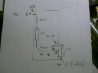
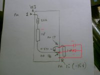
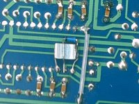
I am gong to do DEM re clock using the Grundig method on Monday hopefully when the diodes arrive - based on the attached.
Can you confirm this will work satisfactorily or is there a better and easier way you can suggest ?
Sorry if this is off topic
Andrew
Hi studiostevus,
When multiple clock loads are connected to the same masterclock output, there is nothing preventing crosstalk between connected clock loads. So a noisy (source) clock load can directly affect a clean (DAC) clock load.
Every logic building block adds jitter, so adding a comparator, buffer, flipflop or gate will result in increased jitter levels.
So you don't suggest flip flop for DEM reclocking ?
.
I am gong to do DEM re clock using the Grundig method on Monday hopefully when the diodes arrive - based on the attached.
Can you confirm this will work satisfactorily or is there a better and easier way you can suggest ?
Sorry if this is off topic
Andrew
Attachments
Andrew,
I will try the Grundig DEM clock solution, but it is not clear what are the capacitor values: 0.1 uF or 1 uF? Also your sketch is different from the Grundig diagram around pin 17. Do you use WS or BCK for DEM clock?
If this works, there is no need to use flip-flops. But the BCK needs to be reclocked in this case...
About the fast Diode
http://www.rfmicrowave.it/catalogo/eng/A.pdf
Could we use the BAR64-02W to replace the BAT 17 ?
http://www.rfmicrowave.it/catalogo/eng/A.pdf
Could we use the BAR64-02W to replace the BAT 17 ?
Last edited:
Hi JustBuildLspkAS,
The balanced masterclock rectifier diodes are most critical, I advise to use HSMS2800 Schottky RF diodes here.
PIN diodes are inferior rectifiers, so I wouldn't advise to use them in this application.
The diodes in the DEM injector circuit are used for temperature compensation and need to have low voltage drop, so that's why I chose Schottky diodes here.
I2S attenuators are based on BAS16 silicon diodes. These are used as rectifier and for temperature compensation.
Could we use the BAR64-02W to replace the BAT 17 ?
The balanced masterclock rectifier diodes are most critical, I advise to use HSMS2800 Schottky RF diodes here.
PIN diodes are inferior rectifiers, so I wouldn't advise to use them in this application.
The diodes in the DEM injector circuit are used for temperature compensation and need to have low voltage drop, so that's why I chose Schottky diodes here.
I2S attenuators are based on BAS16 silicon diodes. These are used as rectifier and for temperature compensation.
- Home
- Source & Line
- Digital Line Level
- Building the ultimate NOS DAC using TDA1541A