Hello John,
Is the 1st quote still a good reference? Or is it override by the 2nd one?
Or can I do a combination? Using SMD per first post then bypass by regular 100nf film capacitor?
Thanks.
Versus
Is the 1st quote still a good reference? Or is it override by the 2nd one?
Or can I do a combination? Using SMD per first post then bypass by regular 100nf film capacitor?
Thanks.
................ When selecting capacitor values with respect to DEM clock ripple current frequency and active divider output current, and using 1uF as maximum value, following would apply:
pin 13,18, 2mA, fDEM /2, 1uF
pin 12,19, 1mA, fDEM, half current (13,18), twice the frequency of MSB, 250nF
pin 11,20, 0.5mA, fDEM / 2, half frequency, half current (12,19), 125nF
pin 10,21, 0.25mA, fDEM, half current double frequency (11,20), 31.25nF
pin 9,22, 0.125mA, fDEM / 2, half current, half frequency (10,21), 31.25nF
pin 8,23, 0.0625mA, fDEM, half current (9,22), 7,8nF
pin 7,24, 0.0625mA, fDEM, equal current (8,23), 7.8nF.
In practice, 1uF (MSB), 220nF, 120nF, 33nF, 33nF, 8.2nF, 8.2nF. This would give equal ripple currents on all MSBs.
Active divider decoupling also depends on DEM clock. Like mentioned before, DEM clock oscillator is able to "lock" on (on-chip) BCK crosstalk. By selecting DEM clock capacitor values that produce (almost) exact multiples of fs, the DEM clock will "lock" to BCK and jitter amplitude would drop significantly. The often used 470pF and 680pF won't result in a "lock" and produce maximum DEM clock jitter amplitude.
........................
Versus
....
10) Use smallest possible 100nF bypass film caps (SMD) and place these underneath the TDA1541A chip for shortest possible connections, every millimeter counts!
........................
Thanks -EC- for your reply (post# 3260)
I understand your remarks. The last DACs I showed are to be used as "portable" units...when I make boxes for them, that is...
The other DACs will use your USB/DI2S receiver whose exact jitter performance has escaped from my memory.
I will search for isachrome and other alloys") Thank you!
Thank you!
I wonder how those alloys "sound".
I have a question: to wind honeycomb coils, with it be detrimental to use some sort of metal (iron; ferrite) nucleus inside?
The thing is that my first attempt with OCC copper wire resulted in only 13 Ohm DC resistance which will give a weak inductance...I can perhaps easily double it, but not too much more...
Nevertheless, I will try those as Power resistors inside a clay mass as an experiment.
Cheers,
M.
I understand your remarks. The last DACs I showed are to be used as "portable" units...when I make boxes for them, that is...
The other DACs will use your USB/DI2S receiver whose exact jitter performance has escaped from my memory.
I will search for isachrome and other alloys
Thank you!I wonder how those alloys "sound".
I have a question: to wind honeycomb coils, with it be detrimental to use some sort of metal (iron; ferrite) nucleus inside?
The thing is that my first attempt with OCC copper wire resulted in only 13 Ohm DC resistance which will give a weak inductance...I can perhaps easily double it, but not too much more...
Nevertheless, I will try those as Power resistors inside a clay mass as an experiment.
Cheers,
M.
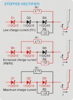
For power supply I now always use 3-stage stepped rectifiers, these greatly reduce (limit) switching noise bandwidth as these offer "soft switching". This has nothing to do with diode type (Schottky) or diode switching noise. Its the effect of switching on / off large capacitive loads like a smoothing cap.
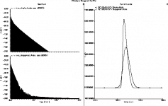
I've simulated the effect of the 3-step rectification, using the values from the published schematic (11D10 schottky diodes, R1=680 Ohm, R2=68 Ohm).
The reduction of spectrum compared to a single step rectification is impressive!
Note that the charge current waveform onset is smoothed, the peak current is reduced, but the pulse is broader compared to the single diode. The integral (=charge) of both peaks is the same.
Rectified voltage is 1.8V lower for the 3-step rectifier and the ripple is the same for both circuits (obviously, since determined by Cmains and Rload).
[test condition: Vsin=15V (amplitude), Cmains=1000uF, Rload=1k]
[circuit diagram: top branch traditional single diode rectifier, bottom branch 3-step rectifier, for head-to-head comparison]
Top circuit, ECdesigns, thanks for sharing.
Attachments
Hi fff0,
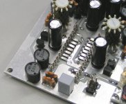
I currently use 14 x 47nF / 16V 1206 size PPS film caps (largest value for 1206 size film cap I could find). These are located underneath the TDA1541A chip and are soldered directly to the pins (shortest possible connection / lowest inductance). I use 2 dedicated GND return paths (L / R channel) that are routed directly to pin 5 and share no other (supply) currents.
I attached a photograph showing how I mounted these SMD film decoupling caps and how I routed GND to pin 5 (AGND).
I now use 1.4112 MHz DEM clock (DEM clock = bit clock), eliminating (on-chip) inter-modulation between DEM clock and I2S signals, and providing extreme low DEM clock jitter as required for maximum performance (bit accuracy).
I didn't use any dividers or flip-flops to drive the DEM oscillator as these add jitter and interference.
DEM clock is injected tapping an approx. 2Vpp square wave signal from the Dynamic Jitter Attenuator circuit. Signal is injected on pin 16 only (pin 17 disconnected) using BAT43 and 12 K Ohm in series (resistor may need fine-tuning). The injector modulates the current on one input of the DEM oscillator, the oscillator now tracks the external DEM clock (can be verified by disconnecting one of the 14 active divider decoupling caps and measuring the signal on the IC pin).
Because the DEM clock rate is approx. 8 times higher than the datasheet application, the 47nF caps are more than effective enough for filtering.
If the DEM oscillator stops (no internal clock signal for the shift registers) massive distortion / hiss becomes audible.
If the DEM oscillator doesn't oscillate or track reliably, low level detail / recordings get distorted.
DEM circuit has significant effect on TDA1541A sound quality, both DEM oscillator and active divider decoupling caps can make or break TDA1541A sound quality as it directly affects accuracy the 6 MSBs.
Is the 1st quote still a good reference? Or is it override by the 2nd one?
I currently use 14 x 47nF / 16V 1206 size PPS film caps (largest value for 1206 size film cap I could find). These are located underneath the TDA1541A chip and are soldered directly to the pins (shortest possible connection / lowest inductance). I use 2 dedicated GND return paths (L / R channel) that are routed directly to pin 5 and share no other (supply) currents.
I attached a photograph showing how I mounted these SMD film decoupling caps and how I routed GND to pin 5 (AGND).
I now use 1.4112 MHz DEM clock (DEM clock = bit clock), eliminating (on-chip) inter-modulation between DEM clock and I2S signals, and providing extreme low DEM clock jitter as required for maximum performance (bit accuracy).
I didn't use any dividers or flip-flops to drive the DEM oscillator as these add jitter and interference.
DEM clock is injected tapping an approx. 2Vpp square wave signal from the Dynamic Jitter Attenuator circuit. Signal is injected on pin 16 only (pin 17 disconnected) using BAT43 and 12 K Ohm in series (resistor may need fine-tuning). The injector modulates the current on one input of the DEM oscillator, the oscillator now tracks the external DEM clock (can be verified by disconnecting one of the 14 active divider decoupling caps and measuring the signal on the IC pin).
Because the DEM clock rate is approx. 8 times higher than the datasheet application, the 47nF caps are more than effective enough for filtering.
If the DEM oscillator stops (no internal clock signal for the shift registers) massive distortion / hiss becomes audible.
If the DEM oscillator doesn't oscillate or track reliably, low level detail / recordings get distorted.
DEM circuit has significant effect on TDA1541A sound quality, both DEM oscillator and active divider decoupling caps can make or break TDA1541A sound quality as it directly affects accuracy the 6 MSBs.
Attachments
Hi maxlorenz,
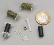
Resistors should have non-magnetic construction. The ISOTAN wire I use is specified as being non-magnetic. The frame is made from CNC milled epoxy or HF PCB material with the copper removed. The core is made from a plastic spacer. The frame is mounted using a nylon M3 screw. I used a brass hexagonal spacer for mounting the resistor to the PCB.
I attached a photograph showing the completed wirewound Mobius / Honeycomb I/V resistors, frame parts and a 1 euro coin for size reference.
The winding starts with folding the resistor wire (making a non-inductive Mobius loop). The center of this loop is fixated to the frame. Now both wire ends are wound onto the frame simultaneously. I skip 3 spokes at a time, with one spoke offset between both wires, creating the honeycomb pattern. When completed, the resistor is calibrated by cutting both wire ends until the value is correct. With the given resistance of 1 Ohm/cm it's quite easy to determine how much wire needs to be cut off.
After calibrating, the wires are fixated to the lower part of the frame using glue. The wires are soldered directly to the PCB in order to minimize the amount of bi-metallic links in the signal path.
This resistor has high wattage, resulting in very low noise. This is essential in order to resolve the LSBs that go down to 61nA fluctuation for the LSB.
The resistor needs to be non-inductive (Mobius loop) and have lowest possible self capacitance (Honeycomb winding pattern) in order to prevent unwanted distortion of the large bandwidth signal, output by the DAC chip.
I have a question: to wind honeycomb coils, with it be detrimental to use some sort of metal (iron; ferrite) nucleus inside?
The thing is that my first attempt with OCC copper wire resulted in only 13 Ohm DC resistance which will give a weak inductance...I can perhaps easily double it, but not too much more...
Nevertheless, I will try those as Power resistors inside a clay mass as an experiment.
Resistors should have non-magnetic construction. The ISOTAN wire I use is specified as being non-magnetic. The frame is made from CNC milled epoxy or HF PCB material with the copper removed. The core is made from a plastic spacer. The frame is mounted using a nylon M3 screw. I used a brass hexagonal spacer for mounting the resistor to the PCB.
I attached a photograph showing the completed wirewound Mobius / Honeycomb I/V resistors, frame parts and a 1 euro coin for size reference.
The winding starts with folding the resistor wire (making a non-inductive Mobius loop). The center of this loop is fixated to the frame. Now both wire ends are wound onto the frame simultaneously. I skip 3 spokes at a time, with one spoke offset between both wires, creating the honeycomb pattern. When completed, the resistor is calibrated by cutting both wire ends until the value is correct. With the given resistance of 1 Ohm/cm it's quite easy to determine how much wire needs to be cut off.
After calibrating, the wires are fixated to the lower part of the frame using glue. The wires are soldered directly to the PCB in order to minimize the amount of bi-metallic links in the signal path.
This resistor has high wattage, resulting in very low noise. This is essential in order to resolve the LSBs that go down to 61nA fluctuation for the LSB.
The resistor needs to be non-inductive (Mobius loop) and have lowest possible self capacitance (Honeycomb winding pattern) in order to prevent unwanted distortion of the large bandwidth signal, output by the DAC chip.
Attachments
Hi jeepee,
Good to hear that you like this circuit.
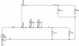
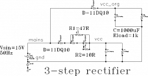
It seems the circuit of the stepped rectifier you attached is wrong, I am not sure if simulations are based on this schematic or on the correct schematics. I attached correct schematics (observe current flow). I wonder how this will simulate.
Top circuit, ECdesigns, thanks for sharing.
Good to hear that you like this circuit.
It seems the circuit of the stepped rectifier you attached is wrong, I am not sure if simulations are based on this schematic or on the correct schematics. I attached correct schematics (observe current flow). I wonder how this will simulate.
Attachments
Hi ecdesigns,
I did the 3-step rectifier slightly different then your schematic, but the basic properties are retained in my implementation.
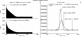
Here are the results for the circuit you posted above (47R, 10R, 3* 11DQ10). I also added the amount of charge in 1 pulse. At 50Hz, this means 50 pulses * 285uC = 14.25mA for the single diode and 50 * 266uC = 13.3mA for the 3-step rectifier. I also plotted the DC load current, 13.05mA. So your circuit wastes less current on higher harmonics or diode charge/discharge. Almost all charge is used by the load!
As for the spectrum, the reduction is quite noticable. Above 20kHz, both rectifiers reach the artificial simulation floor (numerical noise, model inaccuracies etc). Anyway I suppose that beyond -150dB the results are meaningless in practice.
Note: the seemingly solid shape in the spectral plot is actually composed of the first 1000 harmonics of 50Hz...
I did the 3-step rectifier slightly different then your schematic, but the basic properties are retained in my implementation.
Here are the results for the circuit you posted above (47R, 10R, 3* 11DQ10). I also added the amount of charge in 1 pulse. At 50Hz, this means 50 pulses * 285uC = 14.25mA for the single diode and 50 * 266uC = 13.3mA for the 3-step rectifier. I also plotted the DC load current, 13.05mA. So your circuit wastes less current on higher harmonics or diode charge/discharge. Almost all charge is used by the load!
As for the spectrum, the reduction is quite noticable. Above 20kHz, both rectifiers reach the artificial simulation floor (numerical noise, model inaccuracies etc). Anyway I suppose that beyond -150dB the results are meaningless in practice.
Note: the seemingly solid shape in the spectral plot is actually composed of the first 1000 harmonics of 50Hz...
Attachments
Hello John,
Thanks for the quick and detailed explaination.
Now I know what are the decoupling capacitors for and their relation to the DEM clock.
However, in your older post, you are trying to balance the ripple current bying using different capacitance value. But now, its seems that its not needed, may I know why?
Thanks -EC- for your detailed explanation (post #3265).
Maybe I expressed myself wrongly: I was asking about honeycomb inductors (coils) which if built around "air" achieve low inductance. That is why I asked about a metal core...
ISOTAN; ISA CHROME: I am looking for those...
Edit: I found it! It was constantan, not "constantin", John, shame, shame...
Cheers,
M.
PS: I made a chipamp with your stepped rectifier circuit and it sounds very clean! Could not make the AB test because I was on a hurry and now the amp is on better hands...
Last edited:
if properly filtering is usedAccording the Shannon's law theoritecally sampling two times of the maximum frequency of the original signal is enough
44.1-20=24.1khzI think that you have heard intermodulation distortion products created somewhere in the audio chain rather than frequencies beyond > 20kHz.
24.1-20=4.1khz
etc etc etc
Hello Nazar,
I see that you have alot of experience and technical expertise in this area. Furthermore, you have developed your own TDA1541A DAC.
Will it be possible to share with us your implementations? Also what you meant by proper filtering and your resolution for the intermodulation distortion products together with some other ideas/ concept/ solution that you have come out with?
Thanks in advance.
Hello again,
I have completed the dac circuit and trying to make a tonal balance so the filter caps are not finalized yet . In the attached output schematic the capacitor value and the type is something very tricky. I have tried polyester and polypropylene caps . Polyester sounds too metallic and sound is too dry there is almost zero harmonic. So i have tried KP that time mids & highs are quite good but low end is too boomy , the gain get boosted in the lowend . The sound in total is not bad but it needs an improvement in the low frequencies. What can you suggest ? ( I have used 2x 470pF Ero KP caps to get 1nf , because i couldnt find a trusted 1nf MKP or KP capacitor in the electronic market , there are so many noname china caps which i don't rely )
Note : It needs at least 2 days for a new cap to burn & stabilize . So experiments take time
Thanks
Reha
I agree that there are too many experts in this topic but i can see that no one has an idea about which capacitor too choose so i will give the answer of my question
Never use small capacitors for coupling try to use as big as possible . At least bigger than 250V and don't use any china made caps. Wima is the best one . I have replaced the small ERO KP 470pF capacitor with Wima FKP1 1200V 390pF and there is a big difference now . Wima sounds great.
Last edited:
Dear Rehad wrote,
If you look at the thread's title you would recognize that it is about John's DAC. Nobody is forced to answer your question about your own DAC (though I would if I knew what you're talking about).
The best is opening your own thread.
I agree with you: any mod (that involves soldering) would take at least three days of playing to be evaluated.
Good luck,
M
2xTDA1541A NOS Dac Distortion Problem
Hi All,
After reading this thread and some other internet documents i decided to build a 2xTDA1541 parallel DAC, similar to Lesha's DAC. The DAC consists of CS8414 , 2xTDA1541 ( with 100nF decoupling caps ) and for the output buffer there are OPA627 and AD843opamps . It is not a differential dac it's simply a parallel dac.
It tooks me 2 weeks to finish it . When it was complete i have started some listening sessions . The sound was impressive , i could compare it with some hi-end dacs such as Benchmark DAC1 and Reimyo DAP 777 , its sound was fairly good enough . Actually the main difference is that the TDA1541 have a bold sound . It has a deep and tight bass but the highs are a bit rolled off. I was thinking that i have built a good dac until i analyzed its output on the oscilloscope . I have tested the dac using some sine waves starting from 1Khz up to 15Khz . Until 8 Khz it looks fine but after that you have a distorted sine waves . Actually you can see on the scope what you listen . The sound is bold and the signal is bold too. When you magnify this bold signal you can see the distortion . I thought that two TDA1541 are not very well synchronised and there is a timing difference in between. So i have disabled one of it . Single TDA1541 is better but you can still see some distortion above 10Khz. I can't imagine what can cause this distortion . Does anybody has an idea ?
I agree that there are too many experts in this topic but i can see that no one has an idea about which capacitor too choose so i will give the answer of my question
If you look at the thread's title you would recognize that it is about John's DAC. Nobody is forced to answer your question about your own DAC (though I would if I knew what you're talking about).
The best is opening your own thread.
I agree with you: any mod (that involves soldering) would take at least three days of playing to be evaluated.
Good luck,
M
Hello Nazar,
I see that you have alot of experience and technical expertise in this area. Furthermore, you have developed your own TDA1541A DAC.
Will it be possible to share with us your implementations? Also what you meant by proper filtering and your resolution for the intermodulation distortion products together with some other ideas/ concept/ solution that you have come out with?
Thanks in advance.
As far as i know "Nazar" means "Theory" so Nazar mostly shows up in conceptual theory area.
and not one, manyFurthermore, you have developed your own TDA1541A DAC.
see my blog, link in signatureWill it be possible to share with us your implementations?
if you dont want have IMD then you need filter all above 24khz at >90dbAlso what you meant by proper filtering and your resolution for the intermodulation distortion products together with some other ideas/ concept/ solution that you have come out with?
Nazar is my nameAs far as i know "Nazar" means "Theory" so Nazar mostly shows up in conceptual theory area.
Sorry, I did not found the link to your DAC's thread...
Unfortunately i don't have my own thread for this DAC.
It's a perfectly working dac. I decided to put the schematic here for someone who thinks to build a diydac using TDA1541.
Actually burn-in process took a lot of time but now it has a really good sound. I want to encourage everybody who hesitate to start to build a TDA1541 Dac.
- Home
- Source & Line
- Digital Line Level
- Building the ultimate NOS DAC using TDA1541A