Hi all,
Last week Nordic recommended a buffered inv.gainclone solution for my iPod...
Which is Pedja Rogics JFET buffered inverted gainclone.
Then I decided to make that. Because Nordic said a lot of good things about it. He said "the JFET buffer makes too much difrerence". I will use 2SK170 as J2..
Do you agree with him? Do some transistors on input make that much difference? I started to make a PCB for it. And its a bit complex to put them alltogether on one PCB and I dont like many PCBs in one enclosure.
Has anybody tried that circuit before? And is it worth to build?
Thanks a lot.
Last week Nordic recommended a buffered inv.gainclone solution for my iPod...
An externally hosted image should be here but it was not working when we last tested it.
Which is Pedja Rogics JFET buffered inverted gainclone.
Then I decided to make that. Because Nordic said a lot of good things about it. He said "the JFET buffer makes too much difrerence". I will use 2SK170 as J2..
Do you agree with him? Do some transistors on input make that much difference? I started to make a PCB for it. And its a bit complex to put them alltogether on one PCB and I dont like many PCBs in one enclosure.
Has anybody tried that circuit before? And is it worth to build?
Thanks a lot.
Hi there it wont matter much which transistors you use I think, as long as they are largely similar. I think pedja said one could even use 3 of the same type... but just read his site to see if there is any adjustments...
If you read the thread in the solidstate section on the buffer, you would have seen comments by T. who claimed this circuit combined with Pedja's own PSU is one of the best sounding chipamps...
There is a stripboard layout that is quite easy to build and adapt to your component sizes as well as showing right orientation for the fets...
Or if you want I can forward you some basic regulated boards in eagle format... you can always omit the regulator parts and build Pedja's...
Attachments
Hi Dxv,
It's not so much that the buffer improves the signal.
I believe it's more down to preventing the unbuffered signal being ruined by all the wrong (varying) impedances that exist from source to amplifier.
To all our experts,
what does R1 do? Is it there only to attenuate RF?
If so, then I think it would be better before the buffer rather than between the stages.
What does C2 do?
Hi Nordic,
I think I already finish a combined PCB for all.
But I always afraid complex PCBs because of RF interferences etc. I know its too much complex to have a quick examination.
May you have a look pls?
Thx.
I think I already finish a combined PCB for all.
An externally hosted image should be here but it was not working when we last tested it.
But I always afraid complex PCBs because of RF interferences etc. I know its too much complex to have a quick examination.
May you have a look pls?
Thx.
Hi Andrew,
I read Pedja's site a bit. As my understanding, the buffer is for impedance immunity.
And the C2, R1, C1 trio creates a pi filter to reducing ultrasound interferences I guess.
But for all matters I am not sure. Pedja tells more detailed in his site. But my poor English doesnt enable me to get more information.
http://www.pedjarogic.com/gc/index.html
Pls have a check here.
Thx.
I think there is always some luck involved with us beginners...
But it is like horserideing, if you fall off, you must just get on again immediatly... worst case, scenario, you can desolder your parts and build the veroboard version, which works just fine...
I build both channels on the same board, so it is still small and neat..
But it is like horserideing, if you fall off, you must just get on again immediatly... worst case, scenario, you can desolder your parts and build the veroboard version, which works just fine...
I build both channels on the same board, so it is still small and neat..
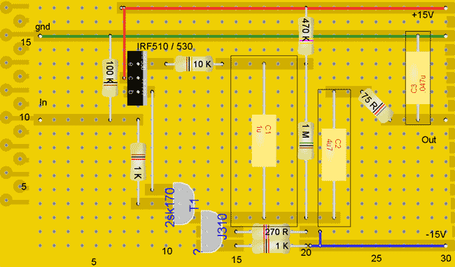
What cap do you intend using for C3?
The shape looks like its for a stacked film resistor. I had a bad experiance of these in my build. (DISCLAIMER: I've only built one, so I'm not an expert). I found that the stacked films I used introduced noise to the signal path and limited my sound.
My suggestion would be to use good quality axial caps such as sonicap, mundorf supreme or similar (there are a few, sonciap VII bypassed by Vishay mkp1837 sounds very good) for this cap. This can be done on the underside of your board perhaps.
Hi Nordic,
You mean you already built that circuit before? So it has to work fine. I am in comfort now!
I will send you the eagle (or gerber) files when it finished. For muting resistor; there is a hidden jumper between two chips mute inputs. Then I put a single 10K via header to Vee. I will use it as a simple and cheap power switch.
I used a four contact relay as power switch in my LM4780 project. However its contatcs got sticked and now I cannot power off my LM4780 GC now.
But I have a question before building that;
I use two 2SK170BL as J1 (the middle one) and J2, one IRF 510 for upper one. Pedja says; you must ommit the R2 if you use 170 for J2. Did you do that? Or what transistor did you use for whole project. For example; Pedja also says "you can use full of 2SK170BL".. Whats the best you think?
And another question; R3 (which is on input) is the bias resistor is it? So 1K is enough I guess. Do you think I am ok?
Thanks a lot.
Dear Justblair,
I dont want to go shopping for that project. Because in Turkey its impossible to find audio grade parts. Even hi quality general parts are not available in Turkey. So I have to order them from US or Taiwan guys for that parts and it gets two weeks at least.
Anyway, I have two alternatives for input coupling cap (C3);
One is Philips 4u7 63v MKP type stock (is what I use for in that PCB)
The other is Changzhou (or like that) brand audio grade 6u8 100v MKT type cap. But I dont trust it too much.
I used that Philips caps (I have a lot of them) in my LM4780 and LM3886 gainclones and I am happy with it. However I use the 6u8 one in my MOSFET amplifier. I cannot say its better than my Philips.
Thanks.
I would not use eletrolitics for these low value caps, as the price on foil caps in these ranges are not too expensive...
Some circuits topologies do use large electrolytics as DC blocking caps... but generaly this is only because you don't get the film caps in high capacities...
Yes I definately built this, and it is my favourite preamp, I did not include all the caps on the output, as I married mine to a My_ref C...
You can see the caps I used from the veroboard layout I posted...
I think I used IRF530, sk170 and J310...
Yep, I also screwed up a $7 relay, which was supposed to be rated high enough... DC is a killer... maybe if you put the relays before the transformer, things could work... but I think it is overkill... I like the datasheet mute pin setup with a cap and resistor giving a little turn on delay, to avoid the turn on thump.
C3 is .47uf
http://www.diyaudio.com/forums/showthread.php?s=&threadid=95007&highlight=
Hi,
yes, all caps leak current from the high voltage side to the low voltage side.
The film caps and similar leak so little it is almost unmeasurable and most manufacturers do not quote any figures.
Paper in oil leak a bit more but it depends on age and history.
Elecrolytics leak a lot in comparison to the low leakage types.
Some electrolytics leak an enormous amount particularly as maximum voltage is approached. The figure quoted by the manufacturer is the typical figure for that model at it's maximum working voltage. Reduce the voltage and the leakage goes down considerably.
Question.
If an Electrolytic degrades with time such that the insulating layer reduces effectiveness to the effect that it reduces the maximum working voltage. This is accepted fact when an electrolytic becomes in need of reforming after operating continuously at low voltage bias.
What happens to the leakage at low voltage as the insulating layer degrades? Does it become worse with time?
Does it become the maximum figure quoted in the datasheets after sufficient time?
Theory is one thing... but in practice my current headphone amp has 1000uf on the output, taken from a motherboard that died after a few years of constant high temp work...it sounds awesome...
to top that the input caps are non-polar elcos too...
Oh and I love paper caps for PSU duty... not so prone to breakdown over time as self healing types...
to top that the input caps are non-polar elcos too...
Oh and I love paper caps for PSU duty... not so prone to breakdown over time as self healing types...
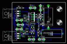
Dear Nordic,
I made some modifications on the amp board that;
I modified PCB for LM3875 because its sound is better as I heard. And the project is mainly designed for it by Pedja. Also I moved the GND point at the middle of PCB. I seperated the signal GND and Power GND via a 470n and 2E2 (in parallel) to prevent noises.
I use two 2SK170 and one IRF510 as recommended and ommited the R2 as also recommended by Pedja.
I designed a special PSU board for hat amp. It includes an output delay circuit onbard.
I purchased the components from Futurlec. I expect the components will arrive in next week. After first try I will send you the eagle files.
These are the new PCBs.
Best regards,
Ozgur
I made some modifications on the amp board that;
I modified PCB for LM3875 because its sound is better as I heard. And the project is mainly designed for it by Pedja. Also I moved the GND point at the middle of PCB. I seperated the signal GND and Power GND via a 470n and 2E2 (in parallel) to prevent noises.
I use two 2SK170 and one IRF510 as recommended and ommited the R2 as also recommended by Pedja.
I designed a special PSU board for hat amp. It includes an output delay circuit onbard.
I purchased the components from Futurlec. I expect the components will arrive in next week. After first try I will send you the eagle files.
These are the new PCBs.
An externally hosted image should be here but it was not working when we last tested it.
An externally hosted image should be here but it was not working when we last tested it.
Best regards,
Ozgur
Looks nice, but while you are waiting, try to split the two boards, can still keep it on same pcb.... so that each channel can receive power from a seperate transformer... for fututre upgrade...
I would also place at least a cap of 100u or so on the output from the 12V reg..
also not that you need a split supply for the pre also...
i.e. +V, -V and 0V....
I would also place at least a cap of 100u or so on the output from the 12V reg..
also not that you need a split supply for the pre also...
i.e. +V, -V and 0V....
- Status
- This old topic is closed. If you want to reopen this topic, contact a moderator using the "Report Post" button.
- Home
- Amplifiers
- Chip Amps
- Buffered IGC. Advice needed.