OK. I'll throw in my view from the bridge of my nose. I dont need the aggrevation of assemblying with SMD. I like to read the part numbers by visual eye and make changes to circuits and change parts etc etc. I am all set up for TH -- auto solder sucker etc. Maybe when I get my eye lens replaced in both eyes. Until then, my vote goes to TH for me.
Most circuits are not so complex that i cant put together a PCB on my own so I have that option, as well.
Drill the holes? Me?
-RM
Most circuits are not so complex that i cant put together a PCB on my own so I have that option, as well.
Drill the holes? Me?
-RM
Drill the holes? Me?
-RM
yes, if you are actually fabricating the PCB at home, with PTH, you need to drill the holes, with SMD (for a simple board like this), very few, just a few vias.
but indeed, PCBs are so cheap now for small runs, you would send it off for proper boards unless you needed it immediately, or wanted to do up a few different variations and be able to try a number of them quickly.
Last edited:
I can understand that SMD design is used when the designer has highly innovative original circuit and wants to prevent people from using it in diy, when his living depends on income earned by the pcb or modules sales. In that case the designer wants to force as many people as possible to buy his pcbs. In that case arguments like "better noise performance", "optimized layout and routing", etc. are used as a kind of FUD strategy. If buyer likes the circuit he does not have other option but to use SMD pcb, or to pay for the assembly. I know that engineers are generally not rich people and that they need money like everybody else. I am not unaware of that fact.
But this is diy site. Most people here are amateurs who have other jobs and want to learn something and have fun. If the designer is interested in selling designs along with pcb's he can earn more money by offering TH pcbs. Offering pcbs with exotic parts that are hard to use by ordinary people is counterproductive strategy. SMD pcbs are toys for higly skilled professionals.
qusp does not understand my argument at all. This is not only about soldering parts, this is about parts that is hard even to see by naked eye, this SMD assembly is watchmakers job.
Last edited:
I will post the final schema up this coming weekend. Then you can critique it and see if you like it - if not, we can tweak it.
I started laying out this past weekend, but it looks like a dogs breakfast, so I scrapped it.
Is this board going to be THP? Makes a difference to how compact we can make it. It's also a whole lot easier to lay out.
I started laying out this past weekend, but it looks like a dogs breakfast, so I scrapped it.
Is this board going to be THP? Makes a difference to how compact we can make it. It's also a whole lot easier to lay out.
Last edited:
qusp does not understand my argument at all. This is not only about soldering parts, this is about parts that is hard even to see by naked eye, this SMD assembly is watchmakers job.
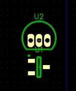
I understand what your argument is, its just not true, especially for this board. I think you have built it up as something that is harder than the reality and think the parts are smaller than they are, as I said, the pad pattern for sot23, is essentially identical in size to that of to92
here they are next to each other. to92 vs sot23 the old 2sk170 low noise jfet staple vs the new bf862 lowest noise jfet staple.
I can see them and solder them with a naked Eye just fine, but for building a large board with 100's of parts like the one I linked above, today 5 years later and nearly 40 years old, to make it easier on my eyes I would use a magnifier, even if only for inspection.
i'm not a watchmaker, its not a watchmakers job, I know people in their late 50's, early 60's working with this stuff just fine. you just need to give it a decent go and dont expect to be as good at it as you are with PTH straight away, it takes practice and new tools (if you want to get serious about it, this little board, I wouldnt bother).
it is not beyond a normal middle to late middle age hobbiest; but many seem to think its beyond them and thats enough to stop them trying, not only that its enough to make them poopoo it and discourage others from trying it, building it up to be harder than it is and spreading this notion so they wont try it either, I dont think this fear-mongering is helpful. this even includes baseless claims of being different sound quality somehow
I find this whole syndrome quite puzzling. you can also use 1206 or 1210 size resistors and caps, or 0508 or 0306 size reverse aspect ratio parts, which give you a larger pad to work with, while still being high performance/low inductance. these again are really not much smaller than a 1/8W PTH resistor
Attachments
Last edited:
SMT seems to be the topic of discussion of late, so I'll ditto what I wrote on the "Discrete OPA design thread" in regard to SMT in general.
If you do the math, I ain't young (54) but god did bless me with being very myopic, which in the case of small, is very good. Must realize that SMT is geared for automated assembly, period.
I have done some big pcb's, where I designed, gave to fab, got an assembled pcb back, with some BGA pkg's used, so it really is the economics of scale. If everything worked, as it should, I did not even have to touch a soldering iron.
Yes as DIY, THT is the best for all concerned, but I want to use a BF862 or one of those duals in a SOT-363? and NXP don't want to bother with a THT pkg, so it is, use what ya got and most possibly limit yourself, or get with the times.
Actually those clowns, finally standardized on the pin out for a bjt/fet in a SOT-23, where as, for say a T0-92, it is scattered about and thus is a PITA.
Awful shame that this SMT issue limits many a man's horizons, so that ends the story for me.
P.S.
In the past, I used a dual footprint, TO-92 (TO-18 staggered) on the top and a SOT-23 mounted on the back side.
If you want to do a better comparison, pair a THT axial R of equiv P with say a 1206 (that is if you do not stand the axial up & use say a SFR16). Must realize that the pcb area costs big?, so limiting pcb area is direct proportional to profit or costs. SMT's, also usually minimize on drill hits, so that saves $ as well. I could go on and on ...
Rick
Last edited:
qusp, let me remind you that I am not running a GB and nobody is going to earn a lot from this one too. But in a recent post in another thread we learned that some forum members are disabled persons who keep solder wire in mouth while soldering with single hand. (Yes, those forum members are ordering pcbs from group buys.) Other forum members are old enough to have problem dealing with tiny SMD parts. If we make THP pcbs all group buyers will be able to build this buffer, not just those who are dexterous and have acrobatic soldering skills.
sorry but thats a strawman argument. are you disabled and needing to hold the solder in your mouth? is that the default position assumed for a DIYer? because there are some small number of hobbiests that are in this unfortunate position, does that mean that everyone must work with only the fast dwindling range of PTH parts left available new? I would hope that this forum being as generous as it often is, if there was members in this position, someone would try and make a PTH layout available for a simple board like this, I would like to think I would.
am I suggesting that PTH should be dispensed with and those who truly cannot manage it be left out in the cold? no, i'm trying to combat the endless stream of excuses why you and others like youm, or really anyone that isnt professional with a mechanised production line or a watchmakers toolset should leave SMD for the robots, because its so small you cant see it and everything is so god damn hard.
PMI, I agree, sorry i'm completely baffled
perhaps I will start a thread regarding this, because I do think its important to try and stop this unfortunate roadblock for the hobby spreading to new members.
Last edited:
I think that would be great. Perhaps we can add some links to your thread on tools, assembly ideas, when you can and cannot use hot air, things like how to store solder paste @ home...... perhaps I will start a thread regarding this, because I do think its important to try and stop this unfortunate roadblock for the hobby spreading to new members.
Yes as DIY, THT is the best for all concerned, but I want to use a BF862 or one of those duals in a SOT-363? and NXP don't want to bother with a THT pkg, so it is, use what ya got and most possibly limit yourself, or get with the times.
Actually those clowns, finally standardized on the pin out for a bjt/fet in a SOT-23, where as, for say a T0-92, it is scattered about and thus is a PITA.
Awful shame that this SMT issue limits many a man's horizons, so that ends the story for me.
P.S.
In the past, I used a dual footprint, TO-92 (TO-18 staggered) on the top and a SOT-23 mounted on the back side.
If you want to do a better comparison, pair a THT axial R of equiv P with say a 1206 (that is if you do not stand the axial up or use a SFR16). Must realize that the pcb area costs big?, so limiting area is direct proportional to profit or costs. SMT's also usually minimize on drill hits, so that saves $ as well. I could go on and on ...
Rick
That would be good compromise if we could make pcb with dual footprint for both TO-92 and SOT. If we manage to make pcb that could use ordinary j-fet, high-end stuff like LSK489 or SOT on the bottom layer. It will require some acrobatics in pcb design. We'll see when Bonsai returns from China if that is possible. We have to finalize circuit before making those decisions. But possibility to use low noise j-fets is highly desirable.
yes, thinking about it, I do think its a really good idea. I wont be able to do all the work and we have some other highly experienced members in this area. we will have to come up with a design that people want to build, something using familiar types of parts, in familiar discrete circuits, but in the 'new' packages. I wonder if the forum would get behind a set of boards listed in the shop? i'm totally up for contributing though, as I spend a lot of time trying to promote the use of the new packages already. mostly I find with the people I manage to get to do it, the major difficulty is in their minds (and I get that btw)
re dual PTH/SMT layout, yep, for a design like this its probably not critical. the dual PTH/SMT pad patterns are more inductive than either one on its own (perhaps a touch more capacitive as well?), so can mess with wide bandwidth designs, but this board and just audio bandwidth I would think its doable. i've used this method before myself, it does usually mean you have to build custom patterns for the parts, but again probably not as much work as doing 2 separate layouts.
it does mean you lose the possibility of having a solid ground plane on the underside, but again here probably not an issue.
@rsavas yeah the alternate to92 pattern with the triangulated pads with the middle pin set forward would match the BF862 better, I just grabbed the nearest one in diptrace for the comparison pic. agreed there is like 4 different pin layouts for to92, only 1 sot23.
Last edited:
Not really so, based on my experience. Did the LSK389 foot print to be able to used SO-8 and T0-72. If I new of BF862, at the time, I'd put that on the back of the proto type. Just a stuffing option, that takes very little room. You are are only going to use 1 of 3 choices, so the pkg's can overlap = no big deal.It will require some acrobatics in pcb design.
A thread on soldering is applicable to everyone on this site or create a sub forum/sticky etc.
I solder DFN's by hand and they are the bitches of them all. Prob is your gotta do i'm first because you need access to a tight space on all 4 sides. Glad most mfg's chose to use DFN over BGA, these days for all but the big pin #'s or I'd/We'd be cooked.
I would be glad to educate the masses, but it is difficult to do so in writing and I ain't running a video recorder set yet.
Today we'll make a pear pie/tarts and write some code

Cheers
Rick
agreed there is like 4 different pin layouts for to92, only 1 sot23.
That is why I called them all clowns!! = PITA,
Political, akin to many politicians, oops
In reality, there is diff smt footprint for wave vs paste/reflow (process), but these guys who build libs for CAD co's do not know much about mfg's, need to refer to ipc etc. Even then you find out how good your pcb is when it comes to time to solder/repair somthing. NXP (Philips) seems to do the best of all the semi mfg at documenting this footprint stuff. okay now it is the end for me on this topic of discussion for this thread.
Last edited:
Hi,
Just recovering from an emergency retinal detachment surgery ..... so I guess that qualifies me to think about SMD a bit.
These few days turned a thread about a cute little circuit into a ridicule
I mean guys we are not talking about fine pitch, TQFN or BGAs here but some of the first SMD device generations here that featured rather smaller casings but not necessarily smaller footprints. Q's comparison of TO92 footprint against SOT23 prooves that easily.
I suggest to decide for SMD or TH after the facts given in #12 and following.
Which is mainly a decision about the required maximum output voltage level and hence required supply voltage range. Going SMD the output is limited to app. 2.5Vrms at +-5V supplies. At this level one might use 6.3V polymere caps like Sanyo Oscon or Panasonics.
Of the suggested JFETs I'd use the 4391 or a similar process 51 device with an Idss around 15-20mA and low Vgs@6-10mA.
The bipolars may be singles in SOT23 or preferrably duals in SOT363, BC847 or 807 or similar. Filtering and DC-blocking caps may be of COG/NPO or film type.
Resistors may be 0805 or 0603 size metal film or thinfilm types.
I'm quite sure that one could source all required devices from a single supplier as digikey, mouser and probabely every second other webshop
Jauuu
now oneeyed Calvin
Which is mainly a decision about the required maximum output voltage level and hence required supply voltage range.
TH is much better choice because we want to use +/-12V rails meaning existing power amp supply. That was part of original "practical" idea. Dropping from 40-50V to 5V will cause too much dissipation in the dropping resisitors, and going for 5V supplies would require separate transformer in which case we could just as well change the original idea and go for buffer that will be used as preamplifier in separate chassis. If we use separate chassis, transformer, series regulation, etc. why not put real preamplifier with gain in it? If we use separate chassis, transformer, regulator, etc. why not relay switching? If we use relay switching why not digital pot? And so on and on....Why complicate the buffer when we could have preamp instead?
- Status
- This old topic is closed. If you want to reopen this topic, contact a moderator using the "Report Post" button.
- Home
- Source & Line
- Analog Line Level
- Bonsai's practical buffer