Waly,
I agree with what you are saying, and at the same time I don't think that counters what I was saying. As long as you take the time constants into consideration you would do just what you are saying. As in any engineering we usually deal with SOA or margins that often are much higher than absolutely necessary but that is just expedient and many times a cover your behind approach to engineering.
I was merely trying to say that not all time dependencies are delays. For the purpose of the thermal system with a massive heat sink, point heat source(s) and a point thermal sensor, it is a delay, though. Such delays can lead to (thermal loop) instabilities, since they introduce a phase lag.
your chassis and transformer are perfect for a very good ClassAB 4ohms capable amplifier.
Just adjust the bias current, using your Oliver criteria, to match the dissipation capability of the sink/s.
5pr biased to 22mVre (100mA bias/pr through 0r22) takes account of some "hidden" internal resistances to give you a dissipation of 10*40V*0.1A + (drivers & predrivers) of around 44W
Assuming the sink has Rth s-a of 0.4C/W, 0.4*44*(DF=1.4) gives a deltaT s-a of around 25Cdegrees. With a Ta=30°C you end up @ Ts~55°C and Tc~60°C which requires the outputs to be derated to ~70% of their cold rating. Even a Tc=70°C (when listening very loud) gives a DF= 0.64
Not a concern since you have a 5pr output stage for a 150W into 4ohms amplifier.
I strongly suggest you build a very current capable PSU to feed the 4ohms speakers.
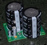
I suggest around +-40mF for each channel, 50V 15mF, 3 to each rail, which for a stereo amp comes to 180mF.
Hi Andrew
Thanks for your detail reply. What is DF?
I have individual pcb holding 2 X 10,000uF 63V, 100uF 100V, 10uF, 100V and 2 X 0.1uF all in parallel for a single rail. This way I make it modualize and scalable so I can put any number of them in parallel to get the amount of capacitance I want. This not only I get scalable capacitance, I have smaller caps in parallel to lower the loss, better frequency response than one or two huge cap.......Not to mention they are cheaper and easier to get.

I might have to consider stacking them up thought as it's taking up space.
I original plan to use 4 of them, one for each rail on each side. I guess I can put more!!
Thanks
Attachments
Last edited:
From my limited experience of testing the beta of transistors, my MJw1302/3281 mostly come within 4 to 5% max of beta matching. Only 4 that is like 20% difference. So if you happen not to encounter the ones that is way off, you might think it's not a problem.
But I am sure if you have one of the transistor that is 20% off, particularly on the higher side, you likely to have problem of hogging.
Larger base stop resistor can make things a lot worst from my calculations here.
I cannot emphasize, matching beta is NOT as hard as people think. I matched over 100 transistor in less than two hours. Don't tell me you have time to talk here and build you dream amp but no time to spend two hours to match the transistors. I have enough transistors to build at least 5 amps for the two hours I spent.
far as I understand, beta matching is the single most important thing to prevent current hogging unless you mess up on the heat sink department.
I don't agree with Self on bolting the bias spreader on the power transistor will prevent hogging. That's apply and orange. Beta matching is the only thing I can think of.......Unless Mr. Cordell tell me otherwise.
Hi Alan,
You are right about the effects of RB exacerbating current hogging. I explained this on page 302 of my book.
I usually use 0.22 ohms RE and 4.7 ohms RB and bias to the Oliver criteria, without thinking very much about it. This is usually adequately conservative and at the same time I am able to get quite low distortion.
In general, if you are worried about current hogging, increased RE and decreased RB will lessen the problem. If you can get reliably stable multi-pair output stages with RB=2.2, that’s great. If you can get away without RB at all, more power to you. However, assuring output stage HF stability under all reasonable conditions can be difficult. This includes at all power levels and with all expected load impedances with all expected phase angles. How low you can go with RB will be a fairly strong function of layout and bypassing.
If you go the ferrite bead or parallel L-R route, you get RB=0 for all practical purposes for DC. This also eliminates any base stopper power dissipation concerns (especially under fault conditions with beta droop). For parallel L-R, which will be linear, recognize that 1uH has reactance of 6.8 ohms at 1MHz. Parallel it with a 6.8 ohm resistor and you have an arrangement that looks mainly resistive for frequencies above 1MHz. That should be more than adequate parasitic protection, since such local HF oscillation problems probably occur at frequencies above 10MHz. You can fit 25 turns of #30 on a half-watt resistor. That gives you about 1.2uH. You can probably fit 17T of #30 on a 1/4w resistor to get about 0.4uH which, paralled with a 4.7 ohm resistor would give you a corner frequency of about 2MHz, which might be OK.
In a multi-pair output stage with temperature sensing on only one transistor, current hogging is not mitigated, so I don’t off-hand know of anything else apart from sufficiently low RB, sufficiently high RE and sufficiently beta-matched output devices to reduce the problem. Note also that if a single sensing device is used only on an NPN device, the PNP devices are left on their own to share equally or unequally whatever the total bias current is.
My equation 15.2 applies to any output transistor sitting by itself in a multi-pair group, at least over the time interval less than the order of the heat sink thermal time constant, which is large, and ignoring the transistor-to-transistor thermal resistance of the heat sink. This also ignores other factors like RB, beta, and internal power transistor ohmic component of effective emitter resistance. I know this is a simplification, and some of these ignored effects will make things worse while others will mitigate the problem. 15.2 gives the first-order insight without boggling the mind.
In my second edition, I will shed more light on output stage stability and how low RB can be chosen to be.
Cheers,
Bob
Hi Alan,
In general, if you are worried about current hogging, increased RE and decreased RB will lessen the problem. If you can get reliably stable multi-pair output stages with RB=2.2, that’s great. If you can get away without RB at all, more power to you. However, assuring output stage HF stability under all reasonable conditions can be difficult. This includes at all power levels and with all expected load impedances with all expected phase angles. How low you can go with RB will be a fairly strong function of layout and bypassing.
In a multi-pair output stage with temperature sensing on only one transistor, current hogging is not mitigated, so I don’t off-hand know of anything else apart from sufficiently low RB, sufficiently high RE and sufficiently beta-matched output devices to reduce the problem. Note also that if a single sensing device is used only on an NPN device, the PNP devices are left on their own to share equally or unequally whatever the total bias current is.
My equation 15.2 applies to any output transistor sitting by itself in a multi-pair group, at least over the time interval less than the order of the heat sink thermal time constant, which is large, and ignoring the transistor-to-transistor thermal resistance of the heat sink. This also ignores other factors like RB, beta, and internal power transistor ohmic component of effective emitter resistance. I know this is a simplification, and some of these ignored effects will make things worse while others will mitigate the problem. 15.2 gives the first-order insight without boggling the mind.
Cheers,
Bob
Hi Mr. Cordell,
Thanks for the detail reply. I am using 2.2ohm base stop. I feel I layout pretty good. I insisted on power and ground planes particular right over the power transistors. I have on the collector of each of the big transistor a 0.1UF in parallel with a 10uF within 0.1" to the collector pin of the transistor. the other side of the caps grounded right to the ground plane. this pretty much getting rid of all the trace inductance of the power and ground. This is my standard cookbook way for EF that I used into UHF range, hopefully this will work for the big transistors here. Layout is everything, I never agree with the idea of not using power and ground plane, with all the parasitic inductance and current loop created by not using planes, then blame on the filter caps(bypass caps) and blame on resonance when parallel a big cap with a small cap.
As for multi stage sensing, I only sense one transistor as I don't want to run traces from the bias spreader all over the place to cover all the transistors. To me, the VAS/bias spreader is quite high impedance and pick up noise and affected by parasitic when running around the board. It is my judgement that it will cause more trouble than it's worth. So I am pretty dead set against sensing all transistors.
From reading the posts here, that the transistors in the middle is going to be hotter and tends to hog current compare to the two at the end. So yesterday, when I burn in the new 0.22ohm for two hours with 3.5A current to cook it good, I measured the voltage drop across each resistor and noted them down ( measuring 0.8V is a lot easier than to measure 0.22ohm direct). The spread is about 2.8%. I then load the lowest resistance ones to the outer most transistor that is not going to get as hot. This will force about 2.8% extra current through the output transistors to heat them up slightly more to balance the temperature. I then slowly increase the resistance of resistors put in as the transistors move towards the center. I put the ones with highest resistance right in the middle transistors.
I am planning to put the transistor with about 1% higher beta on the two ends also to help pulling a little more current from the middle. Then if I sense the output transistor alone, I still get closer to representing the middle. And hopefully prevent hogging.
I cannot emphasis enough that hand pick parts is less troublesome than people realize. As I replied to Waly in detail, if people want just DIY, they sure want to make one better than they can buy on the market, so hand pick should be one of the option. Even if one tries to get into business, one has to have something special to market and sell, hand pick might give the edge.
I cannot emphasize enough that it's not hard to hand pick. I did over 100 transistors in less than two hours including setting up (which take just as long as picking). I can pick enough transistor and match them into sets in one day for a 100 amps!!! How many for the high end amp companies can claim they sell 1000 amps a year?.....Better yet, say 500!!! The bigger the volume of transistor you pick, the less waste you'll have. No matter how far out, you can always match them into sets of even 5 in my case. I bet you can pick a year worth of production in a day or so if you get the routine down. have a good tester, 10 labeled bins. Then you just plug, read and dump into the right bin.
I did understand when reading p300 and 301, the equation is for single transistor where you can use it to anticipate worst case one transistor hogging most current.
Thanks
Last edited:
A. I usually use 0.22 ohms RE and 4.7 ohms RB and bias to the Oliver criteria, without thinking very much about it. This is usually adequately conservative and at the same time I am able to get quite low distortion.
In general, if you are worried about current hogging, increased RE and decreased RB will lessen the problem. If you can get reliably stable multi-pair output stages with RB=2.2, that’s great. If you can get away without RB at all, more power to you. However, assuring output stage HF stability under all reasonable conditions can be difficult. This includes at all power levels and with all expected load impedances with all expected phase angles. How low you can go with RB will be a fairly strong function of layout and bypassing.
B .In a multi-pair output stage with temperature sensing on only one transistor, current hogging is not mitigated, so I don’t off-hand know of anything else apart from sufficiently low RB, sufficiently high RE and sufficiently beta-matched output devices to reduce the problem. Note also that if a single sensing device is used only on an NPN device, the PNP devices are left on their own to share equally or unequally whatever the total bias current is.
C . "boggling the mind".
D. In my second edition, I will shed more light on output stage stability and how low RB can be chosen to be.
I don't mean to "inject" , Bob. But , some of these issues need the "real world" to be worked out properly.
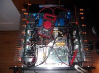
I'm on one week of operation today. No fires , plenty of loud music.
(below) is the unmatched final worst case scenario. Full power -
Tennessee full heating.
A. Your recommendation of .22Re / 4.7Rb works out (adequately).
I have another amp with 2.2Rb that is a little closer. The lower Rb
shows no deviation from the 4.7 - stability wise.
B. On an EF3 with multiple pairs , this is a big problem with only one
sensor. You could sense those 18.7mv or 16.3mv devices in the picture ,
but they do not behave thermally like the other ones. 40C , they are
nearly the same as the other pairs.
The picture sensors are in the middle of the back four outputs , they
sense the "average" of the rear 2 npn's and 2 PNP's.
When I heated this amp up with real (heavy metal
) , the smalldriver extrusion heated in < 1second. It's sensor reacted instantly.
C. This would "boggle the mind" if you tried to work it out with
just pure equations. As an example - the top/bottom C spread of the extrusion
increases between 35C -55C (convection).
D. You might want to examine either an OEM or a sufficiently thought out
DIY design to convey these points. Many of the other DIY projects
on this forum are ignoring these issues , as well as other electrical layout
issues.
PS - by what I'm doing now , I quite sure "it's all worked out" (20+ years
of reliable operation) - before re-capping !!
OS
Attachments
Last edited:
What is what?
If you forgot, it's probably safe for me to forget it too ;-)
I don't mean to "inject" , Bob. But , some of these issues need the "real world" to be worked out properly.
I'm on one week of operation today. No fires , plenty of loud music.
(below) is the unmatched final worst case scenario. Full power -
Tennessee full heating.
A. Your recommendation of .22Re / 4.7Rb works out (adequately).
I have another amp with 2.2Rb that is a little closer. The lower Rb
shows no deviation from the 4.7 - stability wise.
B. On an EF3 with multiple pairs , this is a big problem with only one
sensor. You could sense those 18.7mv or 16.3mv devices in the picture ,
but they do not behave thermally like the other ones. 40C , they are
nearly the same as the other pairs.
The picture sensors are in the middle of the back four outputs , they
sense the "average" of the rear 2 npn's and 2 PNP's.
When I heated this amp up with real (heavy metal
driver extrusion heated in < 1second. It's sensor reacted instantly.
C. This would "boggle the mind" if you tried to work it out with
just pure equations. As an example - the top/bottom C spread of the extrusion
increases between 35C -55C (convection).
D. You might want to examine either an OEM or a sufficiently thought out
DIY design to convey these points. Many of the other DIY projects
on this forum are ignoring these issues , as well as other electrical layout
issues.
PS - by what I'm doing now , I quite sure "it's all worked out" (20+ years
of reliable operation) - before re-capping !!
OS
But if you are running between 14mV to 16mV on the 0.22ohm Re, you are not running very high power at idle. I calculated you are running about 70mA per stage and 350mA total. Assume 160V across total, that's dissipating 56W for the whole amp at idle, as this it mono far as I can see. You have a lot of heat sink for 56W.
But if you are running between 14mV to 16mV on the 0.22ohm Re, you are not running very high power at idle. I calculated you are running about 70mA per stage and 350mA total. Assume 160V across total, that's dissipating 56W for the whole amp at idle, as this it mono far as I can see. You have a lot of heat sink for 56W.
I was just measuring the exposed semi's in a "natural" vertical orientation.
There are two complete AB amps in there. You calculated right , I estimated
>50w per channel.
I'm 144V (not 160).
Alan , I'm the opposite - build it first , then fix it
.Last version favored the middle pairs with abuse. This one is perfect
considering stock unmatched devices.
Edit - those temps. were after I "abused " it.
OS
Last edited:
Hi Bob,
My knowledge has come from years of observing what goes on in the market place. I don't have a problem with DC servo setups as long as they are done properly. Most are not. I will also whole heartedly agree that getting away from that large electrolytic cap is a worthwhile enterprise.
Once I have my stuff back together I'll have a chance to do some poking around on this issue. I am having a problem with the idea that the servo dumping current or voltage into the feedback side of the LTP will not unbalance it. From my viewpoint, that is exactly how the servo works, by forcing the LTP to be out of balance. You might be correct, but at the moment I can't see how that is supposed to work without creating an unbalanced condition.
Bob, can you do me a favor and think about the BGW amplifier example I gave earlier? I can send you the diagram, but it is 7.3 meg in size (full manual). HiFi Engine has it if that is easier. I might need you to type slowly using single syllable words to explain this to me. I just can't see how what you are saying can be true.
Best, Chris
Hi Chris,
There seem to be some misunderstandings about whether a DC servo’s offset correction unbalances the input pair. The short answer is that it does not if the servo correction is applied to the feedback side of the LTP or to the input side of the LTP. It can create imbalance if the servo correction is applied to the current mirror.
The key thing to understand is that when we say an LTP is balanced, we mean that the current though each of the transistors is the same – that is what counts; not the base voltage applied to each device. If the 2 devices are mismatched by 5mV, they WANT to have a 5mV difference across their bases when balanced.
Consider a simple amplifier with an ideal current mirror load and a Darlington VAS so that base current into the VAS can be neglected. The current mirror forces the currents of both transistors in the LTP to be the same, almost no matter what. Else there will be a strong correction that will make its way through the amplifier and back through the feedback network to supply the base voltage to the LTP that will make the currents identical. The DC servo merely supplies a correction voltage to make this happen without resort to an output offset occurring.
You’ve seen more different commercial amplifiers that use DC servos than I have, but my strong impression is that most amplifiers that use a DC servo apply the servo correction to the feedback side of the LTP, so that the DC servo does not create a current imbalance in the input pair.
Note that less sophisticated amplifiers that use a simple resistive load on the IPS instead of a current mirror load will be more susceptible to input pair current imbalance, but this is probably not mitigated or exacerbated by the use of a DC servo.
Cheers,
Bob
My measurements confirm that ThermalTrack diodes still have a delay in responding to temp changes of a few 100 mS. Long term stability may be good, but transient thermal changes are still there.
See my article in Linear Audio Vol 9.
Jan
Hi Jan,
You are exactly right, and that is a very good article. The value of the ThermalTraks is to get the sensing time constant down (faster), but they do not get it down to the point where some effects do not remain. They are by no means perfect.
Note my thermal model of the ThermalTrak transistor in Figure 14.21. This was arrived at by actual measurement of a ThermalTrak device. It models both the junction thermal path and the sensing diode thermal path. The junction time constant is a quite-small 23ms. The case time constant is a moderate 4.5 seconds. The heat sink time constant is a rather large 21 minutes. The “case” node in this model is assumed to be the copper header on which the power transistor die and sensing diode are mounted. The tracking diode adds another 350ms time constant to the temperature of the “case”, reflecting its fairly high thermal resistance to the header because of its insulating epoxy attach.
More interesting is Figure 14.22. Here the sensing diode response time (diode voltage versus time) was measured for four different sensing diode arrangements. The diode voltages were normalized to be the same under the initial condition of no power transistor collector current. Power of 25W was then turned on in the power transistor and the sensing diode voltage was measured as a function of log time.
The four scenarios were: a) ThermalTrak diode; b) TO126 sensing transistor mounted to the surface of the TO264 transistor (the same ThermalTrak power transistor was always used); c) sensing transistor mounted on the heat sink in close proximity to the power transistor; d) sensing transistor mounted 2 inches away on the heat sink.
It is easily seen that the ThemalTrak arrangement is superior to the arrangement where the sensing transistor is mounted to the transistor case. It is also clear that mounting the sensing transistor on the transistor case is superior to just mounting the sensing transistor on the heat sink. Also very interesting is that mounting the sensing diode 2 inches away from the power transistor does not make things hugely worse. At 100 seconds, pretty much in the mid-way point of the fall in sensing voltage, the difference is only 3mV “worse” with the sensing device mounted further away.
At the same 100 second point, the case-mounted sensor is only 10mV “better” than the heat-sink mounted arrangement of (c), while the ThermalTrak is fully 20mV “better” than (c) – twice as good as the case-mounted arrangement.
At 10 seconds, the case-mounted sensor has only moved 2mV from (c), while the ThermalTrak has moved 15mV from (c), showing that the ThermalTrak response is much faster than the case-mounted solution.
Finally, note at 500 seconds the differences in sensing device voltages. Although in fairness the ThermalTrak diode has a somewhat different TCvbe, the other 3 scenarios use the identical TO126 transistor. What this shows is that there are significant differences in thermal attenuation from the junction to the sensing device junction – not just time constant. Figure 14.23 illustrates the large difference in thermal tracking vs time between ThermalTrak and heat-sink mounted solutions on a real amplifier when it has been operating at 50W, dissipating a lot of heat, and the input signal is then removed. The bias was set in this amplifier so that both cases ended up with the same bias at idle.
The test amplifier used an EF Triple with the pre-drivers and drivers mounted on their own heat spreader/heat sink on the circuit board, and their own bias spreader mounted to the heat spreader. The thermal results thus reflect only the thermal dynamics involving the output transistors.
Cheers,
Bob
Hi Mr. Cordell
This is a completely new topic.
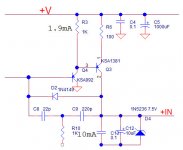
I was reading Feedback Baker Clamp in p367 which I never read before, it got me worry. I put in my anti stick circuit automatically when I design the IPS/VAS board. I just used the standard technique of Schottky TTL idea of using the diode D2 to clamp the base current as shown in the attachment.
When I read your book this morning, I was thinking how come you don't do it like mine as it's so simple. Then I realize I am doing it on the Miller feedback path. I am using 1N4149 with 1pF capacitance. But it is known the reverse diode capacitance change with reverse voltage. This mean I am changing the capacitance a little as the output swing that can cause distortion.
My question to you is whether this is too much that I need to change it? As you can see, I am using TMC with smaller cap 18pF on my board. Is this large enough to swamp out the variation of capacitance of the diode? If I have to modify, this might cause big problem to modify as I don't have a place to clamp to. In Figl 17.3, you use Q11 and Q12 to set up the voltage to clamp to and I don't have it. Please help!!!
Thanks
Alan
This is a completely new topic.
I was reading Feedback Baker Clamp in p367 which I never read before, it got me worry. I put in my anti stick circuit automatically when I design the IPS/VAS board. I just used the standard technique of Schottky TTL idea of using the diode D2 to clamp the base current as shown in the attachment.
When I read your book this morning, I was thinking how come you don't do it like mine as it's so simple. Then I realize I am doing it on the Miller feedback path. I am using 1N4149 with 1pF capacitance. But it is known the reverse diode capacitance change with reverse voltage. This mean I am changing the capacitance a little as the output swing that can cause distortion.
My question to you is whether this is too much that I need to change it? As you can see, I am using TMC with smaller cap 18pF on my board. Is this large enough to swamp out the variation of capacitance of the diode? If I have to modify, this might cause big problem to modify as I don't have a place to clamp to. In Figl 17.3, you use Q11 and Q12 to set up the voltage to clamp to and I don't have it. Please help!!!
Thanks
Alan
Attachments
Last edited:
If you forgot, it's probably safe for me to forget it too ;-)
Oh, "the Plant" in control theory jargon modelling several heat sources and a temperature sensor in the feedback loop has, for all purposes, a "dead zone" that can be modeled as an exp(-Ts) factor in the loop gain. Such an approximate "dead zone" (of course, "pure dead zones" like a step function at t>0 and zero elsewhere do not exist in nature) has the side effect of a phase lag, contributing to the (in)stability of the plant with the closed loop. The farther the sensing transistor, the larger the dead zone. Of course, for the ThermalTrack diode, the dead zone is much smaller and it could indeed be approximated with a more convenient (for analysis) function.
But the important thing is that the thermal stability of a ThermalTrak bias spreader loop is much better compared to a regular bias spreader loop: the lower the dead zone, the lower the phase lag, the better the stability.
why don't you guys just buy a $7 uC with ADC/DAC and use feedforward? - should be very effective in this domain
calc the power dissipation, model the junction temps, adjust the bias - can even continuously identify/update the model
looks like it would be a bit cheaper/easier with a common emitter/floating supply output so all the twiddly sensing doesn't have full range output V swing to diff out
floating the uC on a conventional follower output could also be done
why don't you guys just buy a $7 uC with ADC/DAC and use feedforward? - should be very effective in this domain
calc the power dissipation, model the junction temps, adjust the bias - can even continuously identify/update the model
looks like it would be a bit cheaper/easier with a common emitter/floating supply output so all the twiddly sensing doesn't have full range output V swing to diff out
floating the uC on a conventional follower output could also be done
Then you hang a whole bunch of stuff on the relative high impedance note of the VAS that add capacitance, creating current loop to pick up noise. Connecting the sensor from the output of the big transistor also create a path for signal to feed back to the VAS. Layout is very important, last thing I want is to put a whole bunch of circuits onto this node. It's one thing to draw circuit and theory on paper, it's another thing to implement on a real circuit.
Implementing the uC is easy enough, it's all the complication and potential problems entail with it.
Not only the circuit, you are putting the power supplies onto the node also, more chance of noise. I would not go for that at all.
Want the circuit to be more forgiving in hogging, lower the base stop, put more stages and use higher Re so each run at lower current. Simpler, cheaper and chances of a good layout goes up.
Last edited:
Hi Mr. Cordell
This is a completely new topic.
I was reading Feedback Baker Clamp in p367 which I never read before, it got me worry. I put in my anti stick circuit automatically when I design the IPS/VAS board. I just used the standard technique of Schottky TTL idea of using the diode D2 to clamp the base current as shown in the attachment.
When I read your book this morning, I was thinking how come you don't do it like mine as it's so simple. Then I realize I am doing it on the Miller feedback path. I am using 1N4149 with 1pF capacitance. But it is known the reverse diode capacitance change with reverse voltage. This mean I am changing the capacitance a little as the output swing that can cause distortion.
My question to you is whether this is too much that I need to change it? As you can see, I am using TMC with smaller cap 18pF on my board. Is this large enough to swamp out the variation of capacitance of the diode? If I have to modify, this might cause big problem to modify as I don't have a place to clamp to. In Figl 17.3, you use Q11 and Q12 to set up the voltage to clamp to and I don't have it. Please help!!!
Thanks
Alan
The nonlinear capacitance of your diode is the reason why this type of diode feedback arrangement is not generally used to prevent saturation of the VAS transistor, so it is a concern. I think most amps just let the VAS saturate in clipping. Pick your poison.
BTW, the 2T Darlington VAS brings with it the advantage that the Ccb of the main VAS transistor is not allowed to be fed back to the input of the 2T VAS, so the effect of the nonlinear Ccb of the VAS transistor is nearly eliminated.
Cheers,
Bob
Ha ha, not the answer I am looking for from you. I thought you are all comforting!!
Now what!!! I don't like it to stick. It was so obvious at the time that I totally missed the moon. Got so automatic in prevent the clipping I put it in without even gave it a thought until I read your book today.
most of what you need to measure are low Z nodes, could use optoisolator to get < a few pF to VAS for bias spreader control
whole circuit bootstrapped from the output, could add only few 10s of pF on the output even with small line xfmr
Bob's EC circuitry can be seen as an example of bootstrapped circuitry
I like analog design, but at some point just wanting a result leads me to using today's Big Stick - cheap uC, ADC/DAC, some software
Last edited:
- Home
- Amplifiers
- Solid State
- Bob Cordell's Power amplifier book