I don't think the offset voltage is that important as this is handle by the GNFB.
Thanks
D4....20V zener. But if you meant D2, it drops about 1.9V at 2mA yielding 4mA tail current.
The common type green LED (1.9V @ 2mA) has a tempco to its junction potential almost identical to that of a BJT base junction, making a good voltage reference for a zero tempo current source.
The current sources in you circuit have the transistor tempco canceled with that of the diode the same way. But, using a resistor there in series with the diode subjects you tail current to the power supply voltage fluctuation and low frequency noises. I would never do that unless I have a really well regulated power supply.... perhaps never even I do have a well regulated power supply.
Why do you think the GNFB can and will handle the DC offset? The DC offset I showed in the simulated examples was exactly the result of the GNFB. In a full complementary topology as shown, the input LTPs are not allowed to operate off-balance due to the use of the current mirrors, therefore, the VAS standing current and the output DC offset can and will fall "victim" to component mismatching.
I will not be able to simulate the circuit as you wanted until I get home after work tonight. Did you never put your circuit in a simulator at all? "Common sense" sometimes would not work because what you think ought to be a common sense sometimes could be something that is wrong.
Yes, I read the wrong reference, it's D2.D4....20V zener. But if you meant D2, it drops about 1.9V at 2mA yielding 4mA tail current.
The common type green LED (1.9V @ 2mA) has a tempco to its junction potential almost identical to that of a BJT base junction, making a good voltage reference for a zero tempo current source.
The current sources in you circuit have the transistor tempco canceled with that of the diode the same way. But, using a resistor there in series with the diode subjects you tail current to the power supply voltage fluctuation and low frequency noises. I would never do that unless I have a really well regulated power supply.... perhaps never even I do have a well regulated power supply.
Why do you think the GNFB can and will handle the DC offset? The DC offset I showed in the simulated examples was exactly the result of the GNFB. In a full complementary topology as shown, the input LTPs are not allowed to operate off-balance due to the use of the current mirrors, therefore, the VAS standing current and the output DC offset can and will fall "victim" to component mismatching.
I will not be able to simulate the circuit as you wanted until I get home after work tonight. Did you never put your circuit in a simulator at all? "Common sense" sometimes would not work because what you think ought to be a common sense sometimes could be something that is wrong.
Good point on rail noise, The way I did that is the standard way in IC design when I was designing ICs. The high early voltage of BJT takes care of this. But I know this is not IC design, this is a lot more critical that normal IC.
I still don't see why LED is better than what I use. The diode compensate the Vbe drift with temperature. The more important, I drop 1V across the resistors to swamp out the variation. I am convinced to use ground reference for the CCS rather than going to the rail. But I am still not convinced about the LED.
I use LTspice, but not as often as I should. I just started on the LTspice, but I yet to find the model of different transistors. What simulation you use? Any hint where can I find the model of say BC550 and other power transistors? I was going to start simulation after I sent out the boards as I can change the values any time later.
Hi Mr. Cordell,
Please correct me if I am wrong. I think you short changed yourself in Fig.7.10 when you said the effective load resistance is half the value of R14 in page 139. The reason I said that is because the collector of Q1 and Q2 do not have symmetrical swing ( equal and opposite). The swing of Q2 is limited by Q6,Q13 and R6 to R6/(R1+R2) plus a little bit of the Vbe change of Q6 and Q13. This has a gain of only about 0.5.
But the swing of the collector of Q1 is RL/(R1 + R2) where RL is almost equal to R14. This is because the other side of R14 only swing very little as described above. I did not spend time in doing the exact calculation. It seems in your case, the equivalent load resistance for Q1 should be about say 45K, not 47K/2=23.5K.
Please let me know what you think. This make a huge difference as you almost doubled the gain. Then you can afford to lower R14 to say 22K and still get good gain out of the IPS. This will half the problem of the VAS current variation we have been talking here.
If people use resistor as load for IPS, for R1 and R2 of 470ohm, even if you use 3.3K(max to prevent added distortion according to D Self), the gain of the IPS is only 3.3K/(2 X 470)= about 3.5. I your case, even if you use 12K for R14 and effective resistance is 10K, the gain is going to be 10K/940=10. But difference. Not to mention distortion is a lot lower.
I know the circuit in Fig.7.10 will have some variation of VAS current due to mismatch. That's the reason I up your R5, R6, R7 and R8 to drop one volt. I drop more voltage across R1, R2, R3 and R4 to minimize the variation due to mismatch. BUT to me, ultimately, lowest distortion is the most important thing, I am even willing to hand pick transistors if this is the lowest distortion circuit known. Hell, those small signal transistor are cheaper than dirt. I plan to order 25 or each, maybe I should up it to 50 to hand pick!!!!
Thanks
Last edited:
I still don't see why LED is better than what I use. The diode compensate the Vbe drift with temperature. The more important, I drop 1V across the resistors to swamp out the variation.
You've gotta' be kidding! An LED as voltage reference in a current source cancels out Vbe drift as well as that diode does, it does not suffer from the power supply fluctuation/noise, it drops 1.9-0.6=1.3V over the resistor at emitter, that's whopping 300mV more! More importantly I get multiple power indicators for free! I'd be all sold to an LED.

Last edited:
You've gotta' be kidding! An LED as voltage reference in a current source cancels out Vbe drift as well as that diode does, it does not suffer from the power supply fluctuation/noise, it drops 1.9-0.6=1.3V over the resistor at emitter, that's whopping 300mV more! More importantly I get multiple power indicators for free! I'd be all sold to an LED.
Don't forget you are speaking with an experienced engineer, with
Probably tube based ICs, otherwise I can understand why it is so hard to understand that those resistors across the differential input stage are trading gain for bias stability.30 years of designing RF, analog IC and all different complicated analog electronics
By the same metric, Mr. Stuart is the blue alien from Prometheus visiting us, mortal humans.
You've gotta' be kidding! An LED as voltage reference in a current source cancels out Vbe drift as well as that diode does, it does not suffer from the power supply fluctuation/noise, it drops 1.9-0.6=1.3V over the resistor at emitter, that's whopping 300mV more! More importantly I get multiple power indicators for free! I'd be all sold to an LED.
LED's are cool !
Not only do they negate temperature co-efficient of other stages when used
as a reference/CCS , but with my standard 4 devices (on my input stages) ...
will show many different fault conditions.
Missing rail voltages , insufficient rail to the regulators , "dead" CCS's/cascodes... the LED's tell all .
When all 4 are lit - the amp just freakin' works
!PS - I rely on those handy 1.8 and 3.2V (red and blue) references for
SO many things ... LED fetish
OS
Always have someone like you in the forum.Don't forget you are speaking with an experienced engineer, with Probably tube based ICs, otherwise I can understand why it is so hard to understand that those resistors across the differential input stage are trading gain for bias stability.
By the same metric, Mr. Stuart is the blue alien from Prometheus visiting us, mortal humans.
How consistent is the LED voltage and what is the tempco?You've gotta' be kidding! An LED as voltage reference in a current source cancels out Vbe drift as well as that diode does, it does not suffer from the power supply fluctuation/noise, it drops 1.9-0.6=1.3V over the resistor at emitter, that's whopping 300mV more! More importantly I get multiple power indicators for free! I'd be all sold to an LED.
So your point is you don't need resistor in series with the LED because it drops 1.9V already. So the impedance across the LED is low and I don't need capacitor across the diode resistor to reduce the noise. So I can save components. That I can buy.
Any specific green LED?
Last edited:
Wonderful graphs and plots - here ....
http://www.ecse.rpiscrews.us/~schub...tonics West) Junction temperature in LEDs.pdf
The paper has all the
red (AlGaInP), green (GaInN), blue (GaInN), and ultraviolet (GaInN) plots.
OS
http://www.ecse.rpiscrews.us/~schub...tonics West) Junction temperature in LEDs.pdf
The paper has all the
red (AlGaInP), green (GaInN), blue (GaInN), and ultraviolet (GaInN) plots.
OS
Thank you. I'll read this tonight. At the mean time, I looked at some data sheets of LED http://www.vishay.com/docs/83029/tllg440.pdf. I notice the green LED has the smallest on voltage change when you vary the current around 1 to 2 mA. Is that the reason you guys choose green LED because the voltage is more constant?Wonderful graphs and plots - here ....
http://www.ecse.rpiscrews.us/~schubert/Reprints/2005%20Chhajed%20et%20al%20%28SPIE%20Photonics%20West%29%20Junction%20temperature%20in%20LEDs.pdf
The paper has all the
red (AlGaInP), green (GaInN), blue (GaInN), and ultraviolet (GaInN) plots.
OS
Alan, you have dragged this thread so far off topic, I dare say many of the people subscribed to it have forgotten that it was originally to discuss Bob's book. The problem is that threads like this become impossible to navigate and search.
Why don't you start a new thread to discuss your amplifier and random musings?
Cheers
Christian
Why don't you start a new thread to discuss your amplifier and random musings?
Cheers
Christian
What is re above, 1/gm? If so, it makes sense.
Yes. Sorry, I should have made that more clear.
Cheers,
Bob
Good point, nattawa. So a standing VAS current of 10mA +/- 50%, which seems acceptable to Alan, is asking for trouble, resulting in a highly unstable OPS bias. In such cases, one need a much more robust bias generator than a simple Vbe multiplier. To me, a variation of +/- 50% is totally unacceptable. Better to prevent than to cure. IOW, keep the VAS current as stable as possible.
Cheers, E.
Agreed. +/-50% on VAS standing current is unacceptable.
Cheers,
Bob
I did a quick-dirty simulation again just to show the VAS standing current responding the changes of a transistor in the IPS.
The first picture is before the changes, everything matches, the VAS Ie@Q13 is 4.9mA, the DC offset at output (not shown) is 0.23mV.
The 2nd picture shows one of the current mirror transistors, Q9B, was changed from BC857C (BF=515) to BC860C (BF=315), causing Ie@Q13 to become 2.7mA, and the DC offset at output (not shown) 6.5mV
The 3rd picture shows the current mirror was changed back to where we started, but one of the input transistors, Q5A, was changed from BC847C (BF=524) to BC850C (BF=324), causing Ie@Q13 to become 7.3mA, and the DC offset at output (not shown) 52.3mV.
How do you know it is not Vbe differences. If you want to explore these effects in a controlled way, it is best to keep the transistors the same, but use slightly different models for each one, keeping track of how much the beta or Vbe is different, and changing only one parameter at a time. Alternatively, you can rig the SPICE simulation with an offset voltage source in series with one of the transistor bases.
Cheers,
Bob
Yes, Vbe difference was more than likely part of it, and I don't know by how much, that's why I called it a quick-dirty simulation. Your recommended method of exploring the issue would be a much more accurate and complete one, as it examines one variable at a time in isolation. I once gave this method a thought and asked myself, "then what"? Why not just build this thing with best matched parts I can obtain and see how much of an issue there is in real world. So I decided to go ahead and build it with matched dual transistors, BCM847 and BCM857, at input LTP and current mirrors. I guess that is my way of ducking and getting around a possible problem, and I hope it works out.
Agreed. +/-50% on VAS standing current is unacceptable.
Cheers,
Bob
That's a "broken" circuit.
I complain (look for improvements) at about 10%.
The LIN example from the book is a hard one to beat in the "real world".
(refrigerator to hot room / 40v to 80v rails).
OS
Please, read my website: Super TIS and your questions will be answered.It is not OK for me, I hold onto the design because because each part of the circuit is well proven to have very low distortion. It is more like putting up, making the best and try to make it work.
I studied your circuit more last night, my understanding is you sum/subtract current between both transistors(Q4 and Q5) of the differential pair at the collector of Q9. You pull 5mA using I1 and about 1mA using Q7 to make sure Q10 always conduct current, never turn off. So Q9 operates between almost 1 to 11mA.
Question is what is the distortion? That's ultimately the most important question. This is one part I am not good at calculating. I am still trying to find transistor data for LTSpice to work on the simulation. I am willing to hand pick transistors to match if my circuit is proven to give the lowest distortion. That's what is important to me.
Also in your circuit, the VAS current gain is low, you have to use 5 mA tail current which force you to use 5K input resistance to avoid offset voltage getting too high. Is all the existing preamp able to drive 5K? I don't know, I saw a lot of people use higher input resistance like 25K.
Thank you, lots of reading.Please, read my website: Super TIS and your questions will be answered.
Hi Mr. Cordell,
Please correct me if I am wrong. I think you short changed yourself in Fig.7.10 when you said the effective load resistance is half the value of R14 in page 139. The reason I said that is because the collector of Q1 and Q2 do not have symmetrical swing ( equal and opposite). The swing of Q2 is limited by Q6,Q13 and R6 to R6/(R1+R2) plus a little bit of the Vbe change of Q6 and Q13. This has a gain of only about 0.5.
But the swing of the collector of Q1 is RL/(R1 + R2) where RL is almost equal to R14. This is because the other side of R14 only swing very little as described above. I did not spend time in doing the exact calculation. It seems in your case, the equivalent load resistance for Q1 should be about say 45K, not 47K/2=23.5K.
Please let me know what you think. This make a huge difference as you almost doubled the gain. Then you can afford to lower R14 to say 22K and still get good gain out of the IPS. This will half the problem of the VAS current variation we have been talking here.
If people use resistor as load for IPS, for R1 and R2 of 470ohm, even if you use 3.3K(max to prevent added distortion according to D Self), the gain of the IPS is only 3.3K/(2 X 470)= about 3.5. I your case, even if you use 12K for R14 and effective resistance is 10K, the gain is going to be 10K/940=10. But difference. Not to mention distortion is a lot lower.
I know the circuit in Fig.7.10 will have some variation of VAS current due to mismatch. That's the reason I up your R5, R6, R7 and R8 to drop one volt. I drop more voltage across R1, R2, R3 and R4 to minimize the variation due to mismatch. BUT to me, ultimately, lowest distortion is the most important thing, I am even willing to hand pick transistors if this is the lowest distortion circuit known. Hell, those small signal transistor are cheaper than dirt. I plan to order 25 or each, maybe I should up it to 50 to hand pick!!!!
Thanks
Hi Alan,
I wish you were right, but I don't think so. A good way to evaluate impedance, either in a thought experiment or simulation, is to apply a voltage to the node in question and see what various currents flow. In this case, the obvious current flows through the 47k to the other "diode-connected" side of the current mirror which moves very little. So the current flow is about V/47k. But that is not the only current that flows. The current that flows through the diode-connected side of the current mirror is mirrored over to the other side of the current mirror, to the node we are looking at. This augments the current that flowed through the 47k, and effectively doubles the net current. That is why the impedance ends up looking like about 47k/2.
Cheers,
Bob
I think Nattawa is right.
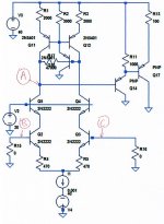
I used LTspice to simulate and experimented to see what is the most sensitive part. Attached is the LTspice schematic file and a JPEG film with points where I measured. I have two schematics, the right side is used as control. I change components in the schematics on the right only.
The main thing I am looking at is point A as this translates directly to the current of VAS. I use only one side of the complementary LTP. The result should be the same with the other side in as it can only add error, it will not subtract even if you think the other side is PNP and reduce the offset. It's the deviation of the offset, not the absolute offset that matters. Here is the result:
1) Q2=Q3=2N2222, R15=R16=25K, point A=37.996V point B=-52.19mV point C=-52.19mV.
2) Q2=2N4124, Q3=2N2222, R15=R16=25K, point A=38.6V point B=-61.5mV point C=-54.5mV.
3) Q2=2N2222, Q3=2N4124, R15=R16=25K, point A=37.4V point B=-54.5mV point C=-61.5mV.
--------------------------------------------------------------------------------------------------------------
Next I grounded the base of Q2 and Q3 to eliminate the offset due to base current:
1) Q2=Q3=2N2222, R15=R16=0K, point A=38V
2) Q2=2N4124, Q3=2N2222, R15=R16=0K, point A=38.32V
3) Q2=2N2222, Q3=2N4124, R15=R16=0K, point A=37.68V
-------------------------------------------------------------------------------------------------------------
Next I test the effect of changing of Q11 and Q12 with Q2=Q3=2N2222. I keep R15 and R16=0ohm to concentrate on the contribution of mismatch of Q11 and Q12 only.
1) Q2=Q3=2N2222, R15=R16=0K, Q11=Q12=2N5401 point A=38V
2) Q2=Q3=2N2222, R15=R16=0K, Q11=2N3907, Q12=2N5401, point A=37.86V
3) Q2=Q3=2N2222, R15=R16=0K, Q11=2N5401, Q12=2N3907, point A=38.125V
Conclusion:
Mismatch of Q2 and Q3 with input resistance of 25K is +/-0.6V
Mismatch of Q2 and Q3 with input grounded is +/-0.32V
Mismatch of Q11 and Q12 with input grounded is +/-0.137V
From the data, I concluded that Q2 and Q3 mismatch is the major problem. Half of the problem is due to the input offset voltage due to the base current.....Which is the Beta difference.
Q11 and Q12 mismatch only contributes relative minor problem.
The result is very discouraging. I am glad I took the time to do the simulation. The only way to reduce the problem is to use
1) Matched pair for Q2 and Q3 as well as the PNP counter part. The match pairs are expensive.
2) reduce the R17 ( R14 in Mr. Cordell's book) to much lower resistance like 10K. but the gain will be reduced.
3) Lower the resistance to the base of the input differential transistors. But that will load down the circuit that drive the power amp. Maybe it's acceptable.
Attachments
Last edited:
- Home
- Amplifiers
- Solid State
- Bob Cordell's Power amplifier book