Waly, I would appreciate your comments about this compensation. http://www.diyaudio.com/forums/solid-state/253039-unique-cfa-120-230w-amp-14.html#post4178869
Damir
You amp's compensation is way to complex to be analyzed by simple inspection. I've counted up to three feedback loops and four poles, then stopped. It appears to be some sort of output inclusive TPC, tamed at HF (where the output stage phase shift starts to be critical for stability) by a lead-lag pole-zero pair.
This would require capturing in a simulator and start analyzing each loop for stability and other properties. I'm afraid I don't have the time to go through this exercise. I have to make a living like everybody else, and audio is not the trade I am, or ever wanted to be, in.
When designing analog circuitry, I tend to avoid doing the whole design in simulator, by patching caps here and there, in an attempt to get something that looks good both in the simulator and as an eye candy. Rather than this mechanical approach, I start by choosing a circuit topology and specifying the required type of frequency compensation that matches a set of end to end requirements (example: I know I can't get more than 40dB of loop gain at 60KHz using Miller compensation, in this particular process, so I have to think about a higher order compensation), then optimize a particular compensation network using the simulator. I also do some rough calculations to find out what would be the maximum feedback for a certain topology (similar to what is described in this paper), just to set the expectations and avoid chasing ghosts.
But I am afraid that such level of design will soon be, at a professional level, a trade of the past (in fact, it already pretty much is). Analog blocks (from op amps to non linear function) are coming in libraries, and the analog designers have to follow more the system design guidelines rather than dealing with low level details like device level frequency compensation. This doesn't mean one can survive while lacking a good understanding of the very basic concepts. For example, when designing a large mixed signal SOC, the overall system stability and the time domain response to input stimuli are usually much more challenging issues than dealing with the details of the op amps compensation.
High level or low level, one thing I learned the hard way is that there are no miracles when it comes to analog design. There is no free lunch, and extraordinary solutions, providing extraordinary performances, are either an illusion, or are disguising a set of trade offs which may not be obvious to start with. Examples from audio: TMC (a two pole compensation in disguise), so-called CFAs (in fact, in particular for audio amplifiers, a circuit topology that trades PSSR, noise, offset, CMRR, loop gain, etc... for speed) and many more examples. There are a few fundamental theorems (Bode, Lurie work on maximum feedback), in fact some sort of "feedback conservation laws", that are guarding up there against any such miracles.
Last edited:
Impressive!!!
Thank you.
Not possible without all the learning and info from all the other wise folks on this forum.
")
What is IIRC? Is CFA and VFA current feedback amp and voltage feedback amp?
I saw a topology suggested by Accuphase that looked like the circuit for those current feedback by the former Comlinear and Elantec amplifiers. I meant to read the article but just too caught up with the tube stuffs lately.
You guys have special acronyms in audio field I don't understand!!!
Here's a primer of sorts on VFA and CFA amplifiers; warning--it's thick with unfamiliar terms and abbreviations, but it's the best article I've found for becoming familiar with current feedback amplifier concepts. The author has designed several such amplifiers which are featured on his Web site:
CFA vs. VFA Amplifiers: a Short Primer
I hope to soon begin building such an amplifier that uses quite a bit of cascoding as well; designed by an engineering acquaintance.
--Damon
Hi Alan,
Much of what you have said is largely true. But as engineers we must pick our poison. And there is plenty of poison to go around in both MOSFET and BJT output stages.
I like MOSFETs because they are fast and are less susceptible to thermal bias problems. But their speed gives them a greater tendency to oscillation.
For a given output stage bias current, much lower THD numbers can easily be had with BJTs. This is due to the lower gm and resulting transconductance droop. Indeed, addressing that problem was why I applied Hawksford error correction to my MOSFET amplifier.
BJTs have also come a long way since then as well. BJT ft is higher and beta droop and ft droop are smaller. The availability of ThermalTraks has made BJTs much more competitive with MOSFETs in the thermal department.
I enjoy working with both technologies.
Cheers,
Bob
Hi Bob, I just read your article "A MOSFET Power Amplifier with Error Correction" from 1984. I read about the Hawksford error correction. It's quite complicated.
So the single source resistor in your book is not good enough to eliminate distortion like the Hawksford error correction? Is that the reason you said BJT works better in low distortion without any compensation?
I am looking at Thermal Track BJTs. My problem is how can I make it work if I have multiple transistor in parallel. But I don't want to trouble you, I already post a new thread here to ask the question.
Thanks
Hi Mr. Cordell,
I have questions regarding to Thermal Track BJT NJL3281 and 1302. In page 306, there is no explanation in what is STTD and TCspread. I can only guess, but are still inconsistency. Can you tell me how to you arrive the value in Fig 14.18?
For Fig. 14.18a, it is quite easy to guess. There is no multiply effect on the TTD1 and TTD2. Seems like the STTD is the multiply factor which is 1.0. The tempco of the MUR120 is -1.7mV, so two of them is -3.4mV. This seems like TCspread is the total tempco of the TTD1 and TTD2.
For Fig.14.18b. Both TTDs are inside the multiplier. So the multiplying factor is 2.1 so the total tempco of the two TTDs is 2.1 X 2 X -1.7mV= -7.14mV, so TCspread= -7.14mV/0C which is close to 7.1mV/0C. The STTD of this is equal to -7.1mV/-3.4mV=2.1.
BUT the numbers in Fig. 14.18c is quite different if I use the same rational. Here, TTD1 is in the multiplier loop and TTD2 is out of the loop. tempco of TTD1 is multiplied by 2.1 which gives 2.1 X 1.7=3.57mV. TTD2 is not multiplied so remains 1.7mV. So the total tempco is -3.57mV - 1.7mV = -5.27mV/0C. So TCspread = -5.27mV/0C. But you gave TCspread = -6.1mV/0C
Consequently STTD calculation is not the same. In your book you seems to use the -6.1mV/-3.4mV=1.8. But if I use my value of -5.27mV, STTD = -5.127mV/-1.7mV = 1.55.
Can you please explain this to me.
Thanks
Hi Mr. Cordell
Sorry to have so many questions. I have another one:
I just read through page 100 to page 103 a few times about gm doubling.
In page 101, it establishes that RE = re'quiescent (5.3)
You use 100mA bias current and choose 0.33ohm for RE to plot the wingspread in Fig. 5.4 which I understand and agree. But then you plot on Fig. 5.5 in page 103 using 100mA AND then increase the current to 300mA to show gm doubling effect. Of cause you see the gm double because you specified you use the same condition, which is still using 0.33 ohm resistor!!! That violates the Oliver's condition in (5.3).
For 300mA, re'=0.087ohm. So the optimal RE = 0.09ohm according to Oliver's. So if I use RE = 0.1ohm, I should not see gm doubling running at 300mA.
I just want to confirm with you on this.
Thanks
Hi Mr. Cordell
Sorry to have so many questions. I have another one:
I just read through page 100 to page 103 a few times about gm doubling.
In page 101, it establishes that RE = re'quiescent (5.3)
You use 100mA bias current and choose 0.33ohm for RE to plot the wingspread in Fig. 5.4 which I understand and agree. But then you plot on Fig. 5.5 in page 103 using 100mA AND then increase the current to 300mA to show gm doubling effect. Of cause you see the gm double because you specified you use the same condition, which is still using 0.33 ohm resistor!!! That violates the Oliver's condition in (5.3).
For 300mA, re'=0.087ohm. So the optimal RE = 0.09ohm according to Oliver's. So if I use RE = 0.1ohm, I should not see gm doubling running at 300mA.
I just want to confirm with you on this.
Thanks
Hi Alan,
Sorry I've been off the radar for the last couple of days. Been dealing with some problems on the homefront. I'll try to get back and answer these questions soon. DIY is a place for ALL of us to learn, both those less experienced and those more experienced. Your questions are important.
Cheers,
Bob
Hi Bob, I just read your article "A MOSFET Power Amplifier with Error Correction" from 1984. I read about the Hawksford error correction. It's quite complicated.
So the single source resistor in your book is not good enough to eliminate distortion like the Hawksford error correction? Is that the reason you said BJT works better in low distortion without any compensation?
I am looking at Thermal Track BJTs. My problem is how can I make it work if I have multiple transistor in parallel. But I don't want to trouble you, I already post a new thread here to ask the question.
Thanks
Hi Alan,
Sorry to be so slow in getting back to you. The Hawksford error correction does add complexity, perhaps 4-6 more transistors depending on your reference starting point for complexity. I think it is fair to say that it eats up some VAS voltage headroom, leading to the desire to employ boosted supplies for the front end of the amplifier. Boosted supplies may be necessary for vertical MOSFET amplifiers anyway, due to their higher Vgs turn-on voltages, often 3.5 - 4V. Indeed, the same may be said about lateral MOSFET output stages. Although their turn-on voltage is much smaller, on the order of a volt, they require quite a bit of Vgs to provide higher output current due to their lower transconductance.
In any case, an amplifier using HEC will be somewhat more complex and expensive.
I have found that the use of source resistors can reduce distortion somewhat
but not nearly as much as HEC. HEC can give you up to 20dB of distortion reduction at 20kHz.
However, TMC compensation of a more conventional MOSFET power amplifier can also provide very significant distortion reduction with very little increase in complexity.
Although I hesitate to make generalizations, a well-designed BJT output stage can usually produce lower measured THD for a given level of complexity than a MOSFET stage. The distortion spectra, thermal effects and some other things may be different, however.
ThermalTrak BJTs are great, and do a lot to mitigate thermal instabilities that can afflict BJT output stages. If you only have a single pair, using both the P-side and N-side diodes is straightforward. Using just one diode of the pair and assuming implicitly that the PNP and NPN thermals behave the same is not quite as good, since low frequency content in music is often asymmetrical and may be within range of the junction/header time constants.
When using more than one pair, I usually think it is OK to assume that all of the NPN junctions will be about the same and all of the PNP junctions will be about the same, so I might just use one diode of each. Of course, one can devise bias spreaders that somehow use all of the diodes in series in a proper way. I don't recall having tried that myself, and am not confident that the possible benefits are worth the trouble.
Cheers,
Bob
Hi Mr. Cordell,
I have questions regarding to Thermal Track BJT NJL3281 and 1302. In page 306, there is no explanation in what is STTD and TCspread. I can only guess, but are still inconsistency. Can you tell me how to you arrive the value in Fig 14.18?
For Fig. 14.18a, it is quite easy to guess. There is no multiply effect on the TTD1 and TTD2. Seems like the STTD is the multiply factor which is 1.0. The tempco of the MUR120 is -1.7mV, so two of them is -3.4mV. This seems like TCspread is the total tempco of the TTD1 and TTD2.
For Fig.14.18b. Both TTDs are inside the multiplier. So the multiplying factor is 2.1 so the total tempco of the two TTDs is 2.1 X 2 X -1.7mV= -7.14mV, so TCspread= -7.14mV/0C which is close to 7.1mV/0C. The STTD of this is equal to -7.1mV/-3.4mV=2.1.
BUT the numbers in Fig. 14.18c is quite different if I use the same rational. Here, TTD1 is in the multiplier loop and TTD2 is out of the loop. tempco of TTD1 is multiplied by 2.1 which gives 2.1 X 1.7=3.57mV. TTD2 is not multiplied so remains 1.7mV. So the total tempco is -3.57mV - 1.7mV = -5.27mV/0C. So TCspread = -5.27mV/0C. But you gave TCspread = -6.1mV/0C
Consequently STTD calculation is not the same. In your book you seems to use the -6.1mV/-3.4mV=1.8. But if I use my value of -5.27mV, STTD = -5.127mV/-1.7mV = 1.55.
Can you please explain this to me.
Thanks
Hi Alan,
This is a hard one to answer on the fly, so I'll have to give it some thought. I haven't looked at that section in about 4 years. Indeed, I also have to make sure that I did not make a mistake. Finally, given your question, it appears to me that I need to do a better job explaining it in the second edition.
Cheers,
Bob
Hi Mr. Cordell
Sorry to have so many questions. I have another one:
I just read through page 100 to page 103 a few times about gm doubling.
In page 101, it establishes that RE = re'quiescent (5.3)
You use 100mA bias current and choose 0.33ohm for RE to plot the wingspread in Fig. 5.4 which I understand and agree. But then you plot on Fig. 5.5 in page 103 using 100mA AND then increase the current to 300mA to show gm doubling effect. Of cause you see the gm double because you specified you use the same condition, which is still using 0.33 ohm resistor!!! That violates the Oliver's condition in (5.3).
For 300mA, re'=0.087ohm. So the optimal RE = 0.09ohm according to Oliver's. So if I use RE = 0.1ohm, I should not see gm doubling running at 300mA.
I just want to confirm with you on this.
Thanks
Hi Alan,
In Figure 5.5 I deliberately over-biased the stage and violated Oliver's criteria to illustrate gm doubling. You are essentially right: with 300mA and reducing RE to 0.09 ohms would bring us back into agreement with Oliver's criteria. The caveat here is that there is some ohmic-appearing resistance in the BJT emitter in addition to the ideal junction exponential part. This can be due to ohmic emitter resistance or ohmic base resistance divided by beta. Base stopper resistors can come into play here, introducing some effective RE that leads to errors in satisfying the Oliver criteria. The relative contribution of these ohmic effects will be larger when using small RE. Note that a 5-ohm base stopper with a transistor beta of 50 will look like ohmic 0.1 ohms as seen looking into the emitter.
Cheers,
Bob
Hi Bob,
Really enjoying reading your fantastic book.
I have a particular interest in the Locanthi Triple T output stage described from p98 onwards and your class AB biasing description. I have build an amp using LJM L25 modules (Triple with 4 pairs paralleled output) transistors and after a few circuit changes it sounds pretty good to me. My question is regarding the optimum output stage idle bias current. The original L25 design was pure class B i.e. no output transistor current though the pre-driver and driver transistors operate in class A. I modified the circuit to allow adjustment of the idle current from 5 - 75 mA. I don't use my amplifier heatsinks as muffin-toasters so I set a fairly conservative 25mA/transistor pair. This is approximately the same total bias as recommended for the single transistor output pair but shared equally for 4 pairs. Does the use of 4 paralleled pairs and the fact that the cross-over distortion is effectively "noise-averaged" by 4 give you a similar THD figure to the single output pair biased at 100mA? What I am trying to understand is that you can get a comparable THD using 4 under-biased parallel transistor pairs instead of one.
Thanks,
steve
Hi Mr. Cordell
I am very grateful you take the time to answer all three of my questions. Bottom line is once I notice I need the HEC, I decided against using MOSFET and move back to BJT. I even decided not to deal with TT transistor and just go back to conventional BJT and use more transistor pairs to achieve the safety margin instead.
From what you said, maybe I should not try to use high bias current like 300mA to avoid the RE to be too low. Is there a lower limit in the value of RE? In another word, the maximum value of quiescent current of each output BJT transistor pair?
Many thanks.
Alan
Last edited:
Where can I find the interviews?Cordell gives details in his "interviews" of how to determine the minimum Re for a particular device and supply rail voltage.
There is a short term stability criteria that must be satisfied.
http://www.diyaudio.com/forums/soli...r-correction.html?highlight=cordell+interview
http://www.diyaudio.com/forums/soli...ive-feedback.html?highlight=cordell+interview
http://www.diyaudio.com/forums/soli...wer-supplies.html?highlight=cordell+interview
http://www.diyaudio.com/forums/soli...jt-vs-mosfet.html?highlight=cordell+interview
http://www.diyaudio.com/forums/soli...ive-feedback.html?highlight=cordell+interview
http://www.diyaudio.com/forums/soli...wer-supplies.html?highlight=cordell+interview
http://www.diyaudio.com/forums/soli...jt-vs-mosfet.html?highlight=cordell+interview
is near the start of this part of the discussion.
Search Thread using Thermal stability and you will see lots of links.
Hi Bob,
Really enjoying reading your fantastic book.
I have a particular interest in the Locanthi Triple T output stage described from p98 onwards and your class AB biasing description. I have build an amp using LJM L25 modules (Triple with 4 pairs paralleled output) transistors and after a few circuit changes it sounds pretty good to me. My question is regarding the optimum output stage idle bias current. The original L25 design was pure class B i.e. no output transistor current though the pre-driver and driver transistors operate in class A. I modified the circuit to allow adjustment of the idle current from 5 - 75 mA. I don't use my amplifier heatsinks as muffin-toasters so I set a fairly conservative 25mA/transistor pair. This is approximately the same total bias as recommended for the single transistor output pair but shared equally for 4 pairs. Does the use of 4 paralleled pairs and the fact that the cross-over distortion is effectively "noise-averaged" by 4 give you a similar THD figure to the single output pair biased at 100mA? What I am trying to understand is that you can get a comparable THD using 4 under-biased parallel transistor pairs instead of one.
Thanks,
steve
Hi Steve,
Once you pick a bias current level for an output pair, satisfying the Oliver criteria is all about choosing the right value of RE. It is understandable if you want to have low dissipation at idle and choose only 25mA, but this just means that you should choose a larger value of RE to satisfy the Oliver criteria. Remember, "under-bias" is a relative thing with respect to what RE has been chosen. In my opinion, it is never good to use a lower RE than called for by the Oliver criteria.
If you are going to run four pair, each at 25mA, and with the appropriate RE for the Oliver criteria, then static crossover distortion will be four times lower, but of course you are now spending 100mA.
Four pairs each run at 6.25mA with the correct RE for that current will likely not perform better than one pair biased at 25mA with the proper value of RE.
Cheers,
Bob
Hi Mr. Cordell
I am very grateful you take the time to answer all three of my questions. Bottom line is once I notice I need the HEC, I decided against using MOSFET and move back to BJT. I even decided not to deal with TT transistor and just go back to conventional BJT and use more transistor pairs to achieve the safety margin instead.
From what you said, maybe I should not try to use high bias current like 300mA to avoid the RE to be too low. Is there a lower limit in the value of RE? In another word, the maximum value of quiescent current of each output BJT transistor pair?
Many thanks.
Alan
Hi Alan,
For practical and thermal stability reasons I would never go below 0.15 ohms for RE. It is just asking for trouble with very little gain. Satisfying the Oliver criteria with that low a value of RE becomes very mushy and inexact, due to the ohmic portion of the emitter resistance of the power transistor.
There is perhaps one exception, and that is in the case of some CFP-type output stages where the thermal stability is less influenced by the output transistor Vbe. However, CFPs have their own set of problems and satisfying the Oliver criteria for them is tough. The Oliver criteria was created in the context of EF output stages, and I'm not even sure it is correct to use that language in the context of a CFP, although one can design and bias a CFP to sort of get the same effect, namely that the net gm of the output stage at idle is about the same as for large currents in either direction. Often, for a "conventional" CFP as found in Self, one has to starve the output transistors (low bias) in order to get the stage to satisfy this criteria. CFP output stages really want to gm-double. I touch on this is my book.
Getting back to EF output stages, I have never built a BJT output stage with RE less than 0.22 ohms.
Cheers,
Bob
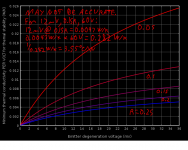
I made a graph to show how degeneration affects thermal stability. It works for any package, insulator, heatsink, voltage, current, Re or Vdegen scenario. You'll have to look at it a bit to figure out how to use it. The thermal resistance you get from this chart is the minimum stable value for Rjh (junction to heatsink), or if you are not using thermal compensation, Rja (junction to room/ambient temp). It is based on the threshold of instability for the thermal circuit. And it may be wrong so it would be nice if someone would check it.
The result given by this chart is the absolute minimum for stability. Even if it's stable, circuits close to the threshold will experience significant thermal drift during operation. So the margin should not be just +20% for instance, but rather a multiple of five or so depending on how much drift is acceptable while the thermal compensation is catching up, and that may be the subject for another chart).
There are exceptions to this behavior. One is an EF stage without paralleled outputs and a Vbe multiplier feedback loop. The Vbe multiplier cancels the tempco of the output bias. However within the feedback delay window, the crossover bias will experience more fluctuation if there is less degeneration. Transistors with built-in thermal diodes for compensation are ideal for this since they reduce the thermal feedback lag.
When temperature feedback such as a thermally coupled Vbe multiplier is used, overall thermal runaway is usually not the main problem. The problem is when multiple outputs are in parallel, because the Vbe multiplier doesn't pay attention to differences between individual transistors. So one transistor will turn off as another one turns on.
Another exception is an output stage with paralleled outputs where each complimentary output pair has it's own thermal compensation loop. This will prevent both thermal runaway and current hogging depending on how well-matched the sensing transistor tempco is to the power transistor tempco.
Attachments
- Home
- Amplifiers
- Solid State
- Bob Cordell's Power amplifier book