Neutralization techniques (cancellation) can help with opening up the OL BW and thus indirectly contribute to lower THD at higher frequencies. But, it can also be useful in preventing or stabilizing the circuit from oscillation with fewer negative side-effects.
Thx-RNMarsh
Thx-RNMarsh
Last edited:
.. for a moment dis SPICE newby thought he would have to resume his fruitless battles with FFT & .four trying to get repeatable results.That is to say, merely the function of providing current gain or changing impedance does not increase open-loop linearity (which is independent of loop gain). However the harmonics introduced by the enhancer may cancel harmonics coming from elsewhere. The point is that the mechanism causing greater open-loop linearity is harmonic cancellation, and that is the answer I gave because you asked the question.
.......
Like I said I will not do it today because I need sleep, but unless you feel my simulations will be an improvement over yours, I suggest you compare the FFT or .four result of the common-emitter base current and the beta-enhancer base current. If I'm right, you will see that the Ib of the enhancer has a smaller H2 than the common-emitter Ib, but not for the 3rd harmonic
As it turns out, the THD is so high for the quantities that kean has asked for, no such subtleties are required
")
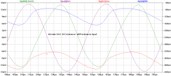
Ib(Q4) & (Q12) are base currents of main VAS & enhancer respectively. As kean suggests, they mostly reflect each other with suitable scaling.
Please note the scaling & arithmetic to get all da plots on the same axes for comparison
But they also show AT THAT POINT, both enhancer and main VAS are mostly VOLTAGE driven. V(n009) is the input to the enhancer which is sorta 'undistorted'.
This is Blameless6 from my #4008 post. 20Vrms 8R 20kHz
If you do the same with the simple Blameless11 circuit with single device BJT, the situation is reversed. Ib(Q4) is sorta undistorted while its base voltage shows the usual Vbe distortion of a CE stage giving clean output current. (looking very like the base currents in Blameless6 in fact)
Here the IPS/CM output is MUCH higher Z than the VAS input so current drive is an 'accurate' description. That makes it MUCH more susceptible to evil VAS Ccb modulation.
With the enhancer in Blameless6, neither enhancer or main VAS are 'purely' voltage or current driven. My example shows more voltage than current but my original assertion that both IPS/CM output Z & VAS input Z are in the same ballpark is probably the best description.
Change of enhancer device, emitter resistor etc can easily swing things slightly to one or the other, making the VAS more or less susceptible to Ccb modulation. But its always less susceptible than Blameless11 when you compensate for Loop Gain and operate at nearly Open Loop as I have done cos 'much more' voltage driven.
__________________
Kean, I'm still interested in your 'hidden distortion cancelling mechanism'. Please don't let my defence put you off finding it.
PS R26 in the enhancer collector is just protection on overload, its position only makes a diff when THD levels of the whole amp falls below 10ppm
PPS IPS CM in both circuits follow Kean's supa dupa recommendations for low distortion CMs with simple circuits.
__________________
Mr. Marsh, please dun insist us beach bums hu neber wen 2 skul cross Bessel functions, triple integrals en udder clever stuff with Guru Wurcer to explain your results
But that doesn't stop us unwashed masses making good use of the phenomena on simple circuits like the Schoeps. We ken pre10 2 B versed in da art
Attachments
@ RNMarsh
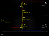
I simmed the following circuit, & used the Jfets shown as i didn't have the ones you did !
Anyway, i found that Without R4 THD @ 1kHz reduced to 0.001% from 0.002%. Increasing the Supply to +- 22V made a Massive difference, as you showed
What a great performance from such a simple & cheap circuit
I simmed the following circuit, & used the Jfets shown as i didn't have the ones you did !
Anyway, i found that Without R4 THD @ 1kHz reduced to 0.001% from 0.002%. Increasing the Supply to +- 22V made a Massive difference, as you showed
What a great performance from such a simple & cheap circuit
Attachments
[Check your SIM models C and be sure they are accurate and not the same value used for both N and P type.]
OK. Here comes the rub for Power Amplifiers and something I am working towards --> As you picked up on... the PS variation makes a huge difference if it changes;
With power amps, the follower type output stage isnt regulated and whether MOSFET or BJT, asymetrical waveforms coupled with high power draw will load down one P.Supply line more than the other and it can be enough voltage drop delta to increase distortion.
And, change THD even more than loading both lines to drop equally, as would be the case with sine wave testing. Its a theory to see what happens in real live circuits.
I would like to see some work on this get SIM'ed, bench tested and published.
Thx-RNMarsh
Last edited:
This bit is WRONG at least in SPICE world. If you check it out with Blameless11, you get more or less the same results as with Blameless6 once you get Loop Gain bla bla out of the way.If you do the same with the simple Blameless11 circuit with single device BJT, the situation is reversed. Ib(Q4) is sorta undistorted while its base voltage shows the usual Vbe distortion of a CE stage giving clean output current. (looking very like the base currents in Blameless6 in fact)
Here the IPS/CM output is MUCH higher Z than the VAS input so current drive is an 'accurate' description. That makes it MUCH more susceptible to evil VAS Ccb modulation.
But this doesn't correspond to my 'real life' experience with this simple circuit though that dates back to 1980 and used really primitive devices. I've looked at Vbe of the VAS under different conditions in 'real life' and simmed it using far cruder methods than SPICE in da old days.
I think the rest of my post is OK. Gotta think hard about the implications.
Anyone know how to reduce Ccb in a SPICE model?
So there IS a 'hidden distortion cancelling mechanism' though I still think modulated Ccb is the major 2nd harmonic mechanism in my examples.Kean, I'm still interested in your 'hidden distortion cancelling mechanism'. Please don't let my defence put you off finding it.
Won't be able to do any serious work on this for a month.
____________________
BTW, this implies that at least at 20kHz, the VAS is a VOLTAGE AMP
So Nyah! Nyah! to da pedants who call it a TIS etc. [deleted 100 pages of rude stuff ]
Last edited:
I've gone through the exercise with Bob's models, sim'ng voltage drops because of real supply impedances; certainly makes a big difference to distortion figures ...
Do you have any examples with numbers to show? To get a feel for the significance of the THD level changes? Is your data somewhere in here?
Often we see talk of THD FFT with stable supplies assumed. Fine assumption for preamps, maybe, but not power amps applied to low efficiency speakers and at high peak levels (dynamics), low Z and high SPL.... in other words.... The real world apps. for PA's.
Thx-RNMarsh
That gave me a question:Blameless11LG.gif is its Loop Gain set so UGLF is 200kHz. A very high Closed Loop gain of 6251x is required for this. At these high Closed Loop gain, such simple circuits don't need any compensation for stability.
If a 25 watts amplifier needs a gain of 34X to support a "right off the DAC" source, then. . . proportionately and without changing the source. . . how many watts amplifier needs the 6251X gain?
I dont think you have to worry about that wit me. use it or loose it. Its lost and I hope I never have to make it come back again.
-RM
Not on the forum, it was just a quick experiment at the time, nothing saved ...Do you have any examples with numbers to show? To get a feel for the significance of the THD level changes? Is your data somewhere in here?
However, just grabbed the TPC model as provided in December, 2010 and tried a simplistic run: 20kHz, 100W, 4R ...
Perfect supplies: 0.00176% distortion
10 mR, only achievable with excellent choice of smoothing caps, and very careful construction: 0.0052%
0.1R, more realistic, much closer to real supplies that would be out there: 0.046%
And this is just assuming a perfect resistance, fed from a perfect voltage - no parasitic inductance, voltage modulation or sag, or other factors ...
The aim of the exercise was to investigate Open Loop THD.That gave me a question:
If a 25 watts amplifier needs a gain of 34X to support a "right off the DAC" source, then. . . proportionately and without changing the source. . . how many watts amplifier needs the 6251X gain?
There are some difficulties doing fair comparisons with Open Loop so I matched Loop Gain at 200kHz cos that's where the THD Analyzer runs out when doing 20kHz THD. The Closed Loop gain for the 2 examples were 6251x & 272728x
Red Book CD is 2Vrms FSD. You'd want 20dB gain in hand for a sensible Volume Control so your amp should clip at 200mV i/p
Blameless6 with 272728x gain could be enlarged to have full output of 0.2x272728 = 85.7dBW (8R load)
THD would be only mediocre but fairly low order.
Not on the forum, it was just a quick experiment at the time, nothing saved ...
However, just grabbed the TPC model as provided in December, 2010 and tried a simplistic run: 20kHz, 100W, 4R ...
Perfect supplies: 0.00176% distortion
10 mR, only achievable with excellent choice of smoothing caps, and very careful construction: 0.0052%
0.1R, more realistic, much closer to real supplies that would be out there: 0.046%
And this is just assuming a perfect resistance, fed from a perfect voltage - no parasitic inductance, voltage modulation or sag, or other factors ...
Those numbers seem realistic and my own similar tests with real live circuits show around a 5-7X or more increase in THD. [give or take... because of this and that].
So this shows up as increased distortion lumped in with other circuit behaviour; Some of it is just caused because the Power Supply has changed its value.
Some of the increase happens when one side of the PS changes relative to the other....but it still happens by about similar amounts in THD when both sides drop as well. Which devices or device parameters are more affected by the PS changes and creating THD in output follower stage? Anyone?
And then, how to minimize the affected parameter. [Other than reg PS for output stage].
Thx-RNMarsh
Last edited:
Originally Posted by RNMarsh
[give or take... because of this and that]
Ahh, this and that, there's an App for that PI 14 Pseudoacoustic Infector
Which devices or device parameters are more affected by the PS changes and creating THD in output follower stage? Anyone?
Well from simming, i've noticed that the lower the resistance of for eg MosFet output devices, the lower THD. P types usually always have higher R than N types, so i guess "maybe" matching N + P by R not I "might" help. Also a balanced Quasi output with matched N types "might" be better ?
And then, how to minimize the affected parameter. [Other than reg PS for output stage].
Possibly configuring a power device in each supply to the Amp, to act as a Cap Multiplier etc ? And/or Active Class A.
Possibly configuring a power device in each supply to the Amp, to act as a Cap Multiplier etc ? And/or Active Class A.
Something like this? http://www.diyaudio.com/forums/solid-state/216780-tt-amp-200w-8ohm-701w-2ohm-2.html#post3115503
@ dadod
Err, not really, as i've never seen that before ! Sure looks an Amp & then some though
I was thinking more like this http://www.diyaudio.com/forums/power-supplies/177516-keantokens-cfp-cap-multiplier.html but a higher powered version, or just a plain 'ol cap multiplier, but HP.
Err, not really, as i've never seen that before ! Sure looks an Amp & then some though
I was thinking more like this http://www.diyaudio.com/forums/power-supplies/177516-keantokens-cfp-cap-multiplier.html but a higher powered version, or just a plain 'ol cap multiplier, but HP.
@ dadod
Err, not really, as i've never seen that before ! Sure looks an Amp & then some though
I was thinking more like this http://www.diyaudio.com/forums/power-supplies/177516-keantokens-cfp-cap-multiplier.html but a higher powered version, or just a plain 'ol cap multiplier, but HP.
There are cap multipliers on each power line with integrated speaker protection.
Okay, sorted. Problem was that the circuit as posted had relatively poor neg PSRR at HF, which was due to the sensitivity of the circuit prior to the output stage. So, regulation or similar, at least here, would resolve this issue ...And then, how to minimize the affected parameter. [Other than reg PS for output stage].
Okay, sorted. Problem was that the circuit as posted had relatively poor neg PSRR at HF, which was due to the sensitivity of the circuit prior to the output stage. So, regulation or similar, at least here, would resolve this issue ...
Please could you provide a link (or post #) to the circuit that you are talking about?
- Home
- Amplifiers
- Solid State
- Bob Cordell's Power amplifier book