PMA said:Simulation is pretty helpful, it enables to subtract output - (input x exact multiple of "steady state" transfer coefficient). The subtraction must be tuned precisely and then you can see what feedback has to control. This is "optimal class B bias" (some 47mA) for lowest distortion NUMBER. Though distortion seems low (like 0.02%), its spectrum is horrible. No real NFB can cure it.
Hi Pavel,
Didn't you say that the emitter resistance was 0.1 Ohm? Self's optimum bias for that resistor value is 215 mA.
andy_c said:
Hi Pavel,
Didn't you say that the emitter resistance was 0.1 Ohm? Self's optimum bias for that resistor value is 215 mA.
I will resimulate for this value. I have tuned the output stage for minimum THD number.
PMA said:I have tuned the output stage for minimum THD number.
Ahh, that explains it. Thanks.
estuart said:The optimal bias depends also on the signal amplitude. So there isn't just one optimal bias for all possible amplitudes.
Yes. Depends on amplitude and load, and probably frequency as well. And it is quite impossible to maintain it.
That is why JC calls for high bias, that is why I design class A stages. Or error corection AB stages, with quite high bias though.
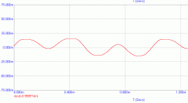
PMA said:this is for 219mA, Re = 0.1, 20Vp, 4 ohm
I do not think it is any better. Again, spectrum is extended far behind audio band.
Hi Pavel,
Is there some attenuation between the voltage source and the EF circuit? The reason I mention this is that the scale factor for the input subtraction is 0.78, which seems low. Seems like it ought to be in the range of 0.9xx or so.
john curl said:No try it with 50ma and .47ohms. This is the normal way of amp design. (not my way )
Here you are
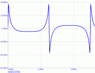
THD of the sole output stage is nice 0.056% at 20Vp/4 ohm. The Fourier spectrum is through whole audio band, with all odd high harmonics quite equal in amplitude.
Attachments
john curl said:No try it with 50ma and .47ohms. This is the normal way of amp design. (not my way )
Hi John,
I agree, 0.47 ohm RE and 50 mA bias is not a very good design, and there are probably too many amplifiers out there with this value. However, I think that the majority of "good" BJT designs are closer to RE = 0.22 ohm and I bias in the range of 100-120 mA.
Cheers,
Bob
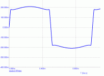
PMA said:Hi Andy,
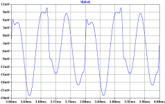
it is like this image. Transfer depends on load, it is 0.91 for 8 ohm and 0.87 for 4 ohm. The coeff I use is tu subtract 1kHz base sine to minimal residual. This depends on amplitude and load.
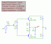
Hi Pavel,
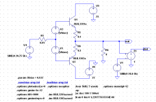
I'm seeing results that are a lot different from this. Schematic is shown below - 25 Volts for Vcc, bias is 0.632 Volts per device for around 215 mA. I use the "dot FOUR" directive, which allows me to see a text representation of the amplitudes and phases of the fundamental and harmonics. I first set the input to 20V peak, then looked at the fundamental of the output. Based on this, I had to readjust the input fundamental to 20.75 Volts to get 20.00 Volts output fundamental component. So this gives me a large-signal gain of 20.0/20.75 = 0.96.
I'll post a zip of the simulation, which will include text files of the MJL1302a and MJL3281a from my web pages
Attachments
PMA said:Well - there is a mistake in 2SA1302/2SC3281 models in MC8. They have emitter resistance of 1 ohm. Andy was right, that is why the gain was so low. MJL models are OK.
Hi Andy,
yes, it was a model mistake, please see above.
Hi Andy,
yes, the same time. The results with MJL1302/3281 in MC8 are quite similar to yours. Anyway, though the subtracted residual does not look so wild now, the Fourier spectrum is still extended high above audio band with high order harmonics quite equal in amplitude. So the task remains the same
yes, the same time. The results with MJL1302/3281 in MC8 are quite similar to yours. Anyway, though the subtracted residual does not look so wild now, the Fourier spectrum is still extended high above audio band with high order harmonics quite equal in amplitude. So the task remains the same
- Home
- Amplifiers
- Solid State
- Bob Cordell Interview: Negative Feedback