This circuit came about from designing industial battery chargers and also electrical power meters and uses a PIC micro with 10 bit A/D to monitor the current through the emitter resistors and the voltage accross the output devices.
Peak detection is important taking into account that the current and voltage is not in phase. The micro drives two (LED = SCR) opto couplers which when fired will latch and disable the MOSFET gates until power is removed and restored.
You could do very much the same using op-amps as comparators and set the trigger point where the voltage and current remains in the safe area. This would be a more general purpose application as the phase information would be difficult to obatain from such a simple circuit.
Although the microprocessor circuit is very simple, the software is not that staright forward and the algorithms is proprietry software of the company I work for, but I think I have given the general idea and there will be some software buffs in the formum that could make this a project.
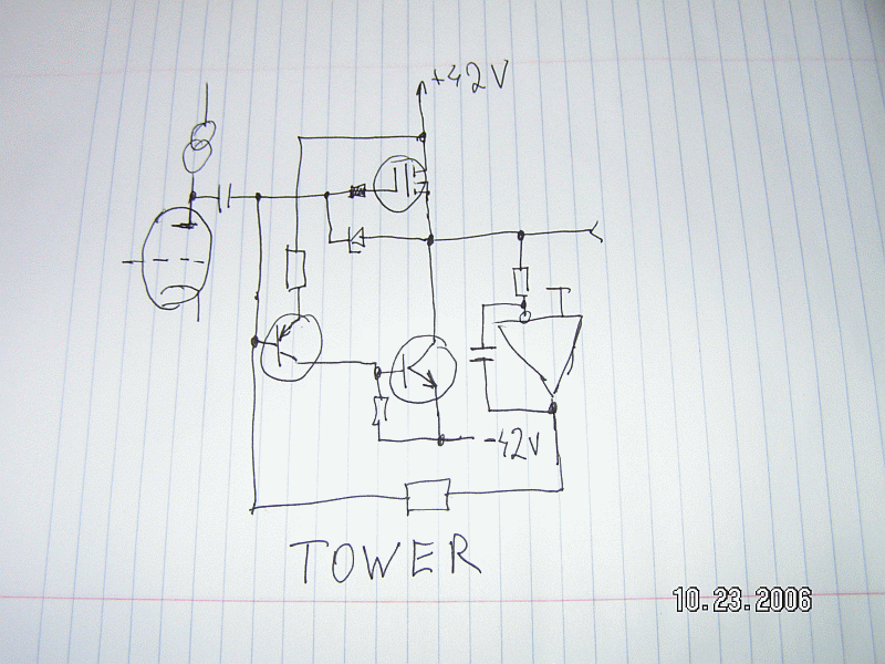
note that the ground of the micro is -V because the A/D cannot go negative. Attached is a block diagram.
Peak detection is important taking into account that the current and voltage is not in phase. The micro drives two (LED = SCR) opto couplers which when fired will latch and disable the MOSFET gates until power is removed and restored.
You could do very much the same using op-amps as comparators and set the trigger point where the voltage and current remains in the safe area. This would be a more general purpose application as the phase information would be difficult to obatain from such a simple circuit.
Although the microprocessor circuit is very simple, the software is not that staright forward and the algorithms is proprietry software of the company I work for, but I think I have given the general idea and there will be some software buffs in the formum that could make this a project.
note that the ground of the micro is -V because the A/D cannot go negative. Attached is a block diagram.
I will draft you the full schematic over the week-end and post it here. The circuit is very straight forward, but I cannot share the software with you as it uses some proprierty algorithms.
In brief you monitor the voltage across and current through the output device then calculate the instantaneous power from that. You can then decide if the power lies under the SOA curve or exceeds your output that would drive two separate opto couplers which is intended to drive the power supply switches.
I would assume that one could also use crowbars to intentionally blow the power fuses of the amplifier that is running into problems, there are a few options. I used electronic relays which essentially are constructed using power FETs.
The ten bit PIC micro has 4.88 mV resolution if referenced to 5V. The killer of transistors are low frequency and running the micro at 20 - 40 Mhz is sufficient.
If you write efficient software and sit in a tight loop monitoring the voltage and current, you can take a measurement on a port (8 x I/O) every few uS, thus sampling eight output devices at speeds exceeding 100 kHz.
Based on the efficiency of your code and your sample rate, you can decide what SOA curve you want to follow.
If you want to improve the measurement resolution you can also employ amplifiers before the A/D ports, but I did not find this necessary at the time and never bother to re-visit the design. At the time I also used an analog port to determine the heatsink temperature and the ambient temperature using NTC that decided to kick in a fan when necessary.
I was anticipating a sliding bias to keep the amplifier running a cool class A but never got that far because pressures at work took was more impoertant. I am taking leave tomorrow until New Year and may put some effort into this but it is not on my list of priorities.
You could most likely achieve a similar SOA protection solution using op-amps but you will have only a threshold and that may not be accurate because the current may be out of phase with the voltage and may have to use a wider gaurd rail thus kicking in the circuit before it is really necessary.
Here I am speculating because I have not used an op-amp for the purpose I will try a few ideas to see if this is feasible and if it is I will gladly post what I have tried and there may be others on this forum that can improve on it.
Kindest regards
janneman said:Hey, Rodent,
Give us a break! The comparator is not the issue, the issue is to combine the Ire and Vce is such a way that it models the SOA. If you have a circuit for that, that would be VERY great!
Jan Didden
mikeks said:
Okay here is a small document with circuit and a functional description attached.
I asked for the schematic on the basis of your claim that you have a working system. This is obviously not the case.
I see notice that the mute realy part is not complete as described, there should be 100 ohm inserted between the NC terminal and -V so that a voltage divider is formed by the speaker resistance and the 100 ohm when muted. Is this description Okay?
Hello
I am new in the diyforum but I have fully read this interesting thread.
I would like to ask Mr Cordell and Mr Curl and all of you how do you rank the Locanthi topology of BJT CC output transistors certainly with respect to class A drivers and low ouput impedance drivers in front of the final stage.
Do you see possibility/benefit to use MOSfet in the output pairs
The use of the ONsemi thermaltrack transistors in a Vbe multiplier together with .3 to .5 resistors in the emitter will make a very effective tracking and thermal stable topology.
Another question is: if we use a front end like the LM4702 with the potential of huge desensitivity in the audio band, then the Locanthi toplogy must leave very little distortion: will a mosfet pairs or BJT pairs make a difference in quality in this configuration
As a final question: is the use of ONsemi thermaltrack, Locanthi topology and LM4702 not the best fit for a DIY needing a top solution with low headache in the 100w+ range?
A question to M Cordel: I see reference to the so called gm doubling and even gm doubling distortion. If you read the explantion of Leach it seems very logical that this is not existing, what do you think?
Last question but perhaps not pertaining to this thread:
In the LM4702 apl. note, it looks like the input coupling capacitor is making a difference in sound not the operating conditions of the output stage ( then what with gm distortion ?). To avoid the use of capacitors, a servo amp is the cool solution, do you have experience with potential drawbacks of servo use?
JPV
JPV said:Locanthi topology of BJT CC output transistors
As in James Bart Locanthi sound ?
Don't you just mean a triple darlington aka T-Rex ?

JPV, when the T circuit was first published about 40 years ago, it was ahead of its time. Many people here use a complementary darlington triple, and some even use a stepped power supply. However, we are discussing details and distortion mechanisms that are more subtle than what the T circuit resolved, or we would all use it today.
The ON semi thermal tracking parts could make a really good class B amp, such as a car amp, better. However with a class A-B amp, there is only a small advantage of instant stable idle current, rather than stable idle current after warm up.
IC's are not what we usually find as the ultimate drivers for output stages.
In my opinion, Gm doubling really exists, and only can be smoothed by voltage drive and the proper value emitter resistors for a given idle current. Usually, too high a value resistance is used for an emitter resistor and Gm doubling then becomes important.
Hi,
Your observation seems to point to Vre being in need of optimisation. This also, by co-incidence or otherwise, comes very close to D.Self's view that both Gm doubling exists and that voltage across the bias resistors is the appropriate method of setting up the output stage. Or am I reading too much into your comment?
is there a way to identify the correct Iq and Re?john curl said:Gm doubling really exists, and only can be smoothed by voltage drive and the proper value emitter resistors for a given idle current. Usually, too high a value resistance is used for an emitter resistor and Gm doubling then becomes important.
Your observation seems to point to Vre being in need of optimisation. This also, by co-incidence or otherwise, comes very close to D.Self's view that both Gm doubling exists and that voltage across the bias resistors is the appropriate method of setting up the output stage. Or am I reading too much into your comment?
JPV said:Hello
I am new in the diyforum but I have fully read this interesting thread.
I would like to ask Mr Cordell and Mr Curl and all of you how do you rank the Locanthi topology of BJT CC output transistors certainly with respect to class A drivers and low ouput impedance drivers in front of the final stage.
Do you see possibility/benefit to use MOSfet in the output pairs
The use of the ONsemi thermaltrack transistors in a Vbe multiplier together with .3 to .5 resistors in the emitter will make a very effective tracking and thermal stable topology.
Another question is: if we use a front end like the LM4702 with the potential of huge desensitivity in the audio band, then the Locanthi toplogy must leave very little distortion: will a mosfet pairs or BJT pairs make a difference in quality in this configuration
As a final question: is the use of ONsemi thermaltrack, Locanthi topology and LM4702 not the best fit for a DIY needing a top solution with low headache in the 100w+ range?
A question to M Cordel: I see reference to the so called gm doubling and even gm doubling distortion. If you read the explantion of Leach it seems very logical that this is not existing, what do you think?
Last question but perhaps not pertaining to this thread:
In the LM4702 apl. note, it looks like the input coupling capacitor is making a difference in sound not the operating conditions of the output stage ( then what with gm distortion ?). To avoid the use of capacitors, a servo amp is the cool solution, do you have experience with potential drawbacks of servo use?
JPV
You've asked a lot of good questions. I agree with John in what he has said in his reply. Most designers would do very well, even today, to use the Locanthi T circuit in driving either bipolar or MOSFET output stages. It does a very good job of isolating the VAS from the output transistors.
I think better approaches to thermal tracking and bias setting are always desirable, but I have no experience with the OnSemi Thermaltrak transistors.
I think the general conclusion of this MOSFET vs Bipolar thread is that very good amplifiers can be made with either technology, and that it is mainly a matter of which device's peculiarity the designer wishes to face and conquer. I'll probably continue to use MOSFETs and John will probably continue to use BJTs. If you look in the commercial high-end market, you will find extremely well-reviewed amplifiers representative of both BJT and MOSFET output stages.
GM doubling is very real, but it is a matter of degree, and proper design and biasing can mitigate it. The use of a number of paralleled output pairs appropriately biased helps. On the other hand, if you use a conventional CFP output stage with 0.33 ohm emitter resistors, and bias the output stage at, say, 100 mA or more, and drive a 4-ohm load, you'll definitely see the effect. In the crossover (Class-A) region, the output stage output impedance will be about 0.16 ohm, while outside this region the impedance will be 0.33 ohm (neglecting inherent output impedance of the stage for simplicity - it will be small). This leads to a 4 percent change in voltage gain into the 4-ohm load, which will, of course, create distortion. Note that the edges where this output stage transitions from Class A to Class B will be fairly sharp, as well.
I do not subscribe to Self's GM-doubling-phobia, however, and believe that his approaches to biasing can lead to under-biased output stages under some conditions. If you err due to the realities of thermal mis-tracking, you want to err on the side of having more bias than optimal (as long as you don't get the output stage too hot).
I use dc servos all the time so as to avoid the capacitor issue you mentioned. I use an inverting integrator with an inverter. Although this takes two op amps instead of just one, I like it better. Don't make the mistake of using crappy op amps in the d.c. servo. I set the gain back to the injection point at the input stage to be fairly small, permitting the servo to only adjust for about 100 mV of offset. This further minimizes the influence of the servo on sonics.
Cheers,
Bob
john curl said:....
IC's are not what we usually find as the ultimate drivers for output stages.
....
John,
I should personaly benefit from elaboration on this assertion from yours.
Being aware at least of a couple of limitations - thermal coupling and lack of suitable complementary devices within the same process, I am quite satisfied with high performance IC's as front ends provided loading is kept within capabilites and the power stage has some voltage gain.
Rodolfo
john curl said:
In my opinion, Gm doubling really exists, and only can be smoothed by voltage drive and the proper value emitter resistors for a given idle current. Usually, too high a value resistance is used for an emitter resistor and Gm doubling then becomes important.
Another obvious solution: single ended class A output stages, but in such case you'll loose advantages against tubez, in terms of power consumption.
Ingrast, I have IC's that I have collected and used for the last 40 years, in my lab. None, to the best of my knowledge, will do as good, much less better than a good discrete design for the input stage of an audio power amp.
There are good reasons for this, because Bob Cordell and I, for example, can use j-fets that are not available to IC designers. I use complementary fets in every input stage that I design. No IC has them.
IF you are happy with IC's, then use them.
There are good reasons for this, because Bob Cordell and I, for example, can use j-fets that are not available to IC designers. I use complementary fets in every input stage that I design. No IC has them.
IF you are happy with IC's, then use them.

At audio frequency a discrete implementation will always be able to have higher performance than an IC. This is because the discrete designer is able to choose devices from basically any process she wishes, wheras the IC designer is stuck wih the process they'll be making the IC with.
Further, a discrete implementation can be much better tailored for a given application than an IC, as an IC generally has to suit a wide range of applications.
This isn't always so though. Often discrete implementations are crippled because their designers oversimplify them. There's a definate "less is more" mantra that does the rounds here. Less is more only when it doesn't degrade performance.
One of the things that always gives me mirth is reading reviews of the gaincard amplifier, where the reviewers go on about the tiny number of parts on the board (nine, I think). They neglect to mention the couple of hundred parts hiding in the amp IC.
At really high frequencies (where interconnect parasitics become important) then sticking everything on an IC has enormous advantages. Audio is not high frequencies though (with the exception of the front end of your tuner).
At all frequencies, there are also clearly cost benefits. It's a lot cheaper and easier to use one IC rather than a hunded or more discrete devices.
Regards,
Suzy

Hmm... What about hybrid ICs? I heard some institute in St Petersburg put vacuum tubes in them...
Aren't they even making some kind of micro tubes directly on silicon nowadays? They are probably quite different in behaviour from ordinary tubes, though.
Wavebourn said:Hmm... What about hybrid ICs? I heard some institute in St Petersburg put vacuum tubes in them...
Hybrids let you use discretes in a design while forgoing many of the parasitics that plague them. You lose the leadframes and many of the PCB parasitic capacitances. Of course you've still got wirebonds to contend with, and it's just as expensive to make as a fully discrete design.
This is stuff that's interesting at gigahertz. Not at audio frequencies, where parasitics matter much less.
Regards,
Suzy
Concerning gm doubling
Mr Cordell, in case of complementary feedback pair it is perhaps right but in emitter follower pair like in the T topology, I do not understand gm doubling.
If you read the paper from Leach (http://users.ece.gatech.edu/~mleach/papers/classab.pdf) on gm doubling it seems undeniable with spice simulation, analytical demonstration and an explanation why the misconception .
He uses two matched transistors which is certainly not true in a real life but the argument remains.
If this is true, then the T circuit is really great not only because it loads very lightly like any darlington but also because the drivers are allways in class A ( emitters not connected to the load but between themselves through a resistor) makes them a very good low impedance to suck the charges out of the output stage. This is very good to reduce the remaining crossover spikes.
M. Curl, I understand that this topology is 40 years old but is it not the same for all of them
I am in the process of learning and I would love to understand what are the subtle distortion mecanismes that still exist in the output stage and how to solve them ( except layout of course)
When I say IC I mean front end like the LM4702. Experienced designers can certainly design discrete high voltage gain stages with good desensitivity and stability which is given for free by the LM4702 in the 100W+ ( I am not selling for National !!).
Mr Curl, what do you dislike in a specific IC like this one driving an output stage in this range of power
If all this is true, ( for the diy) making a medium power amplifier boils down to choosing between BGT and MOSfet for efficient reliability and protection mecanism. With use of servo and bridging, he can make a very high power with a BGT/MOSfet choice for ease of paralleling.
Mr Cordell, why do you prefer inverting servo and where can I read on the use of servo to remove offset.
Many Thanks to all of you
Jean-Pierre Vanderreydt 🙂
JPV said:.....T circuit is really great not only because it loads very lightly like any darlington but also because the drivers are always in class A.....
Depends on the size of cross-coupling resistors; if small enough, then all drivers in class A.
JPV said:.....where can I read on the use of servo to remove offset.
Here.
- Home
- Amplifiers
- Solid State
- Bob Cordell Interview: BJT vs. MOSFET