Speaking of valves, I'm thinking about putting a valve pre in this amp (mostly just for the novelty) as a guitar amp, can you think of any problems with using across the entire secondary (~70Vpeak) doubler to get me up to about 140Vpeak?
Haha and yeah I'm 24, so those amps are probably before my time...
Haha and yeah I'm 24, so those amps are probably before my time...
Speaking of valves, I'm thinking about putting a valve pre in this amp (mostly just for the novelty) as a guitar amp, can you think of any problems with using across the entire secondary (~70Vpeak) doubler to get me up to about 140Vpeak?
Haha and yeah I'm 24, so those amps are probably before my time...
Just thinking quickly... a doubler doesn't actually double the AC voltage as such, it gives an output equal to double the DC value a normal rectifier and cap would give. Helps if you see it drawn.
Voltage doubler - Wikipedia, the free encyclopedia
Grounds... the SS amp is on a split supply. The "ground" of the doubled output isn't the same point and they can't be tied together.
Why not just use a simple FET preamp to give the same type of harmonic distortion as a triode instead.
Yeah sorry maybe I wasn't clear; the transformer I'm using is about 25-0-25Vac, so it gives +/-35Vdc rails when rectified. If I used the double across the entire secondary winding (~50Vac which would give ~70Vdc rectified) I should get close to 140Vdc?
The grounding issue is one thing that definitely occured to me, but I don't necessarily see why it would be a problem. The low voltage at the bottom of the cathode resistor of the tube wouldn't be at the 'ground' voltage at the centre of the reservoir capacitors, but is that a problem? It would act as ground for the valve section of the circuit which would be cap coupled to the next SS section, so DC voltages are removed anyway. Does what I'm saying sound like it makes sense or am I missing something?
The grounding issue is one thing that definitely occured to me, but I don't necessarily see why it would be a problem. The low voltage at the bottom of the cathode resistor of the tube wouldn't be at the 'ground' voltage at the centre of the reservoir capacitors, but is that a problem? It would act as ground for the valve section of the circuit which would be cap coupled to the next SS section, so DC voltages are removed anyway. Does what I'm saying sound like it makes sense or am I missing something?
Best if you draw it out.
Cap coupling the audio is no problem. The grounds are. The SS uses the centre tap ground as an absolute reference for audio signals (input ground, feedback ground, speaker return). The valve stage will use what ? The lower end of the cathode resistor ? That would be the normal point that all the valve stages would use as their reference point for ground returns etc.
As the two grounds, SS and Valve are at different potentials what do you do ?
I see what you mean now Mooly, simulated it and found that you were correct. You can use a doubler to produce two nodes with a constant doubled voltage across them, but they will be oscillating relative to the ground voltage of the rest of the circuit, so the quiescent voltage of the tube stage would also be oscillating relative to the ground voltage... Looks like I'd need a separate transformer or to just run the tube stage off the 70Vd between the +/- rails.
Thanks for pointing that out, I couldn't get my head around the concept until I simulated it.
Thanks for pointing that out, I couldn't get my head around the concept until I simulated it.
Blameless style amp redesign and build
Hopefully this isn't considered reviving an old thread. I took your advice with regards to Pdiss in the VAS and CCS transistors, and used better output devices in a 2channel rebuild of this project. The power supply is now a 35-0-35V, 300VA toroid giving about 51v rails unloaded, powering both channels. Power devices are mounted on a large fan assisted heatsink rated at 0.6degC/Watt without fan and 0.3degC/Watt with the fan. There are no signs of instability driving reactive loads (2uF cap across 8R resistor), and whilst I haven't yet accurately tested distortion I expect it to be small.
The amps are now putting out about 135W each into 8R, but are limited by the single slope VI limiting to about 150W into 4R purely because I didn't want to use two pairs of output devices per channel (although the boards do have provision for this) and the transformer is rated at 300VA.
The only things I dislike are the fan noise, which isn't a huge issue as I only turn on the fan when playing so loud the fan noise can't be heard, and the fact that in negative clipping some small oscillations are seen, I'm not exactly sure why?
Thoughts, comments, opinions welcome.
Attachments
Yeah it was with no load. It looks like ringing in the high audio band only on the negative clip.
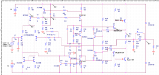
The return of the zobel has its own separate return to the star ground, as do the on board reservoir caps (100uF and 100nF) which I forgot to include in the schematic.
Feedback is taken from a separate tee off the main output track.
D3 and D4 are actually 3A 400V types, forgot to mention that.
The return of the zobel has its own separate return to the star ground, as do the on board reservoir caps (100uF and 100nF) which I forgot to include in the schematic.
Feedback is taken from a separate tee off the main output track.
D3 and D4 are actually 3A 400V types, forgot to mention that.
I ran some THD tests with ARTA software; I first directly looped the soundcard and tested THD with averaging to get a benchmark, then ran the loop through the amp into a passive buffer consisting of a pot and some clipping diodes to protect the input of the soundcard. The output was set to 8.9Vrms (10W into 8ohms) for most of the tests and the buffer was used to attenuate it to exactly the same output as the soundcard's output voltage (1Vpk-pk).
I then subtracted the THD found for the soundcard alone from the THD with the amp in the loop to get a measure of the amp's THD.
1kHz, Amp unloaded: THD: 0.0006%, THD+N: 0.0001%
1kHz, 8R Load (10W): THD: 0.0004%, THD+N: 0.0004%
1kHz, 4R Load (20W): THD: 0.0008%, THD+N: 0.0015%
2kHz, Amp unloaded: THD: 0.0005%, THD+N: 0.0001%
2kHz, 8R Load (10W): THD: 0.0003%, THD+N: 0.0004%
2kHz, 4R Load (20W): THD: 0.0002%, THD+N: 0.0015%
5kHz, unloaded: THD: 0.0008%, THD+N: 0.0002%
5kHz, 8R Load (10W): THD: 0.0005%, THD+N: 0.0003%
5kHz, 4R Load (20W): THD: 0.0002%, THD+N: 0.0003%
10kHz, unloaded: THD: 0.0001%, THD+N: 0.0001%
10kHz, 8R Load (10W): THD: 0.0034%, THD+N: 0.002%
10kHz, 4R Load (20W): THD: 0.0041%, THD+N: 0.0022%
Unloaded 28.3Vrms @1kHz: THD: 0.0003%, THD+N: 0.0001%
Obviously the results are pretty questionable; in many cases the THD+N is lower than the THD which I can't explain, and in many cases the THD into a 4R load is less than that into an 8R load, which could possibly be due to the amp being under-biased and the extra heat generated with the larger currents causes Vbias to come closer to the optimal value.
The results at 10kHz are particularly unreliable because my soundcard is on 16bit, so pretty much all harmonics after the second would be cut off.
Despite all this I'm happy with the results as they suggest the amp is producing less than 0.0009% THD, at least below 5kHz.
Any comments regarding the measurement method and results are welcome!
Cheers.
Thoughts, comments, opinions welcome.
Can you explain me the function of this further LP filter R13-C2?
You have already TPC, so stability should be already achieved
Call it as you like, but it is a further pole in the transfer function, with a further 90 degree phase shift that comes along. So you better make sure that the gain is already under 0 dB when this pole takes place, otherwise your phase margin.....Wouldn't C2 and R13 actually be lead compensation? As an aside, it seems to me that TMC works better than TPC. Connect R25 to the output instead of the -V rail to see if you get some improvement.
BTW I am NOT criticizing this design in general, that for my taste is one of the absolute best that I have seen in this forum.
Last edited:
Yes it is also lead compensation, in my build (actually used 100pf and 1nf for TPC), sims seem to suggest that its not necessary for stability, it probably would be if I reduced those values though.Wouldn't C2 and R13 actually be lead compensation? As an aside, it seems to me that TMC works better than TPC. Connect R25 to the output instead of the -V rail to see if you get some improvement.
Self also suggests that swapping the compensation caps can reduce the VAS loading problem that comes along with TPC, so I might try that.
At the moment there's a bit of ringing on square wave, but it seems entirely stable with any load I've tried including capacitative ones.
These are some of my favorite designs also, I don't know why TPC seems so unpopular here.
Yes it is also lead compensation, in my build (actually used 100pf and 1nf for TPC), sims seem to suggest that its not necessary for stability, it probably would be if I reduced those values though.
Self also suggests that swapping the compensation caps can reduce the VAS loading problem that comes along with TPC, so I might try that.
At the moment there's a bit of ringing on square wave, but it seems entirely stable with any load I've tried including capacitative ones.
These are some of my favorite designs also, I don't know why TPC seems so unpopular here.
Take a look at the thread "TMC or TPC my dilemma resolved?"
http://www.diyaudio.com/forums/solid-state/188133-tmc-tpc-my-dilemma-resolved.html
dado
Ugh, realized why I was seeing so much ringing on the square wave response: because I was using my 16bit soundcard as a signal generator which produces a square wave with hell of a lot of ringing already. Tried it with an analogue square generator and there is almost no ringing/ overshoot at all.
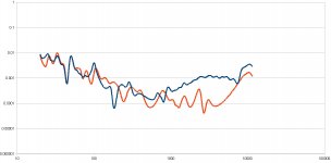
Also, for anyone who's interested I've been playing around with the STEPS program that comes in the ARTA bundle; I measured stepped sine response for the amp with and without the TPC resistor connected to V-, (effectively comparing single pole comp. and TPC). I exported the results to excel and subtracted the values for the soundcard alone as before and charted them. Again, I wouldn't say this method is accurate to any great degree but it does show the expected improvement with TPC compared to single pole comp.
The orange trace is for TPC, the blue trace is single pole. The lines have been artificially smoothed slightly also to make them a little clearer.
There seems to be an increase in distortion at LF which I'm not sure about; whether or not it's actually present or just an artifact produced by the soundcard measurement method.
These tests were run at 10W into 8R (resistive load).
Attachments
Last edited:
I do not think so.With regard to R13/C2 and R14.
I think R14/C2 put a zero near 1Mhz (presumably the cross-over F) for some added phase margin and the R13/C2 pole rolls off this zero at a much higher frequency ~48Mhz (using the values shown)
Hope this helps
-Antonio
In your hypothesis, the gain of the ampli first rises at low freq. (at the zero) then levels off with the pole at a higher gain value.
A simple asyntotical analysis tells you that the gain is first high at low freq.
(circa= 1 + R14/R12 , then decreases at the pole, then levels at the zero at a lower value (circa=1 + (R14//R13)/R12 ,that can be approx. to 1+R14/R13).
So first comes the pole and then the zero.
Last edited:
.....................that can be approx. to 1+R14/R13).
QUOTE]
Sorry, I mistyped. I meant final gain 1+R13/R12 in the last formula.
- Status
- This old topic is closed. If you want to reopen this topic, contact a moderator using the "Report Post" button.
- Home
- Amplifiers
- Solid State
- "Blameless" style ~100W amp with CFP output.